An oxide semiconductor just single atom thick
A new study, affiliated with UNIST has introduced a novel method for fabrication of world's thinnest oxide semiconductor that is just one atom thick. This may open up new possibilities for thin, transparent, and flexible electronic devices, such as ultra-small sensors.

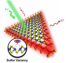
The above graphic displays the growth of ZnO on graphene layer, consists of interconnected hexagons of carbon atoms. Zinc atom shown as red spheres, oxygen atom as green spheres.
UNIST

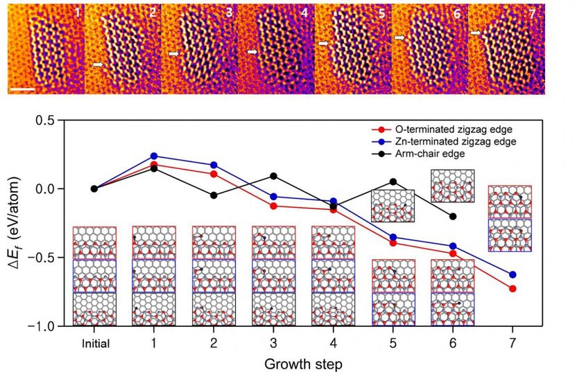
Figure above shows the lateral growth of the ZnO monolayer along the zigzag edges.
UNIST


This new ultra-thin oxide semiconductors was created by a team of scientists, led by Professor Zonghoon Lee of Materials Science and Engineering at UNIST. In the study, Professor Lee has succeeded in demonstrating the formation of two-dimensional zinc oxide (ZnO) semiconductor with one atom thickness.
This material is formed by directly growing a single-atom-thick ZnO layer on graphene, using atomic layer deposition. It is also the thinnest heteroepitaxial layer of semiconducting oxide on monolayer graphene.
"Flexible, high-performance devices are indispensable for conventional wearable electronics, which have been attracting attention recently," says Professor Lee. "With this new material, we can achieve truly high-performance flexible devices."
Semiconductor technology continually moves toward smaller feature sizes and greater operational efficiency and the existing silicon semiconductors seem to also follow this trend. However, as the fabrication process becomes finer, the performance becomes much critical issue and there has been much research on next-generation semiconductors, which can replace silicon.
Graphene has superior conductivity properties, but it cannot be directly used as an alternative to silicon in semiconductor electronics because it has no band gap. A bandgap gives a material the ability to start and stop the flow of electrons that carry electricity. In graphene, however, electrons move randomly at a constant speed no matter their energy and they cannot be stopped.
To solve this, the research team decided to demonstrate atom-by-atom growth of zinc and oxygen at the preferential zigzag edge of a ZnO monolayer on graphene through in situ observation. Then, they experimentally determine that the thinnest ZnO monolayer has a wide band gap (up to 4.0 eV), due to quantum confinement and graphene-like 'hyper-honeycomb' structure, and high optical transparency.
The currently-existing oxide semiconductors have a relatively large bandgap in the range of 2.9-3.5 eV. The greater the band gap energy, the lower the leakage current and excess noise.
"This is the first time to actually observe the in situ formation of hexagonal structure of ZnO," says Hyo-Ki Hong of Materials Science and Engineering, first author of the paper. "Through this process, we could understand the process and principle of 2D ZnO semiconductor productiom."
"The heteroepitaxial stack of the thinnest 2D oxide semiconductors on graphene has potential for future optoelectronic device applications associated with high optical transparency and flexibility," says Professor Lee. "This study can lead to a new class of 2D heterostructures including semiconducting oxides formed by highly controlled epitaxial growth through a deposition route."


