New silicon-germanium nanowires could lead to smaller, more powerful electronic devices
Microchip manufacturers have long faced challenges miniaturizing transistors, the key active components in nearly every modern electronic device, which are used to amplify or switch electronic signals.
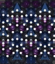
Now, researchers from the UCLA Henry Samueli School of Engineering and Applied Science, Purdue University and IBM have successfully grown silicon-germanium semiconducting nanowires for potential use in next-generation transistors.
These nanowires — which measure from a few tens to a few hundreds of nanometers in diameter and up to several millimeters in length — could help speed the development of smaller, faster and more powerful electronics, according to study co-author Suneel Kodambaka, a UCLA professor of materials science and engineering.
"We are excited for two reasons," said Frances Ross, manager of IBM's Nanoscale Materials Analysis department and corresponding author of the study. "One is that we have extended our knowledge of the fundamental physics of the process by which nanowires grow. The other is the improved prospect of using nanowires in high-performance electronic devices."
"The nanowires are so small you can place them in virtually anything," Kodambaka said. "Because of their small size, they are capable of having distinctly different properties, compared to their bulk counterparts."
The team showed they could create nanowires with layers of different materials, specifically silicon and germanium, that were defect-free and atomically sharp at the junction — critical requirements for making efficient transistors out of the tiny structures. The "sharper" the interface between the material layers — in this case, just one atom, or close to one atom, thick — the better the electronic properties.
"We think this study is significant because it provides a solution to the problem of growing sharp interfaces in nanowires, thereby addressing an important limitation in the growth of nanowires," Ross said.
According to Kodambaka, silicon-germanium nanostructures also have thermoelectric applications, in which heat is converted into electricity.
"The Jet Propulsion Laboratory uses bulk chunks of silicon-germanium to power their satellites, and now there is a lot of interest in using a similar technology in automobiles. These nanowires have great potential in any area involving electronics," Kodambaka said.
To grow the silicon-germanium nanowires, tiny particles of a gold-aluminum alloy are first heated to temperatures above 370 degrees Celsius and melted inside a vacuum chamber. A silicon-containing gas is then introduced into the chamber, causing silicon to precipitate and form wires under the droplets. A germanium-containing gas is used to form the germanium wires.
"Think of it as ice growing from water vapor or the formation of ice crystals during a snow storm. You can get forests of ice wires under the right conditions instead of getting snow flakes or flat films of sleet," Kodambaka said. "But instead of water vapor, we introduced silicon vapor to get the silicon wire."
"The challenge was to create a really sharp interface between the silicon and germanium in each wire," Kodambaka said. "So we cooled the liquid droplets until they solidified. This allowed us to get rid of excess silicon in the alloy. Then, germanium wire segments could be grown on the silicon with the introduction of germanium vapor, and sharp interfaces formed."
The next step for the team is to grow the same structures over larger areas in a conventional growth reactor rather than in a tiny area under the microscope.
"This will allow my colleagues at IBM to process the wires into devices and measure their electronic properties," Ross said. "Of course, we would hope that the properties are improved, compared to conventional nanowires; and if this works out, we will look into new devices and try out different metal alloys to determine which is best for making devices."
Original publication: Science, Nov. 27, 2009

