X-ray snapshot of butterfly wings reveals underlying physics of color
A team of physicists that visualized the internal nanostructure of an intact butterfly wing has discovered two physical attributes that make those structures so bright and colorful.

Scales from the wings of the Emperor of India butterfly consist of “highly oriented” photonic crystals.
Photos by Andrej Singer, UC San Diego
"Over millions of years, butterflies have evolved sophisticated cellular mechanisms to grow brightly colored structures, normally for the purpose of camouflage as well as mating," says Oleg Shpyrko, an associate professor of physics at UC San Diego, who headed the research effort. "It's been known for a century that the wings of these beautiful creatures contain what are called photonic crystals, which can reflect light of only a particular color."
But exactly how these complex optical structures are assembled in a way that make them so bright and colorful remained a mystery. In an effort to answer that question, Shpyrko and Andrej Singer, a postdoctoral researcher in his laboratory, went to the Advanced Photon Source at the Argonne National Laboratory in Illinois, which produces coherent x-rays very much like an optical laser
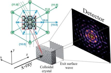
By combining these laser-like x-rays with an advanced imaging technique called "ptychography," the UC San Diego physicists, in collaboration with physicists at Yale University and the Argonne National Laboratory, developed a new microscopy method to visualize the internal nanostructure of the tiny "scales" that make up the butterfly wing without the need to cut them apart.
The researchers report in the current issue of the journal Science Advances that their examination of the scales of the Emperor of India butterfly, Teinopalpus imperialis, revealed that these tiny wing structures consist of "highly oriented" photonic crystals.
"This explains why the scales appear to have a single color," says Singer, the first author of the paper. "We also found through careful study of the high-resolution micrographs tiny crystal irregularities that may enhance light-scattering properties, making the butterfly wings appear brighter."
These crystal dislocations or defects occur, the researchers say, when an otherwise perfectly periodic crystal lattice slips by one row of atoms. "Defects may have a negative connotation, but they are actually very useful in improving materials," explains Singer. "For example, blacksmiths have learned over centuries how to purposefully induce defects into metals to make them stronger. 'Defect engineering' is also a focus for many research teams and companies working in the semiconductor field. In photonic crystals, defects can enhance light-scattering properties through an effect called light localization."
"In the evolution of butterfly wings," he adds, "it appears nature learned how to engineer these defects on purpose."
Most read news
Topics
Organizations
Other news from the department science

Get the chemical industry in your inbox
By submitting this form you agree that LUMITOS AG will send you the newsletter(s) selected above by email. Your data will not be passed on to third parties. Your data will be stored and processed in accordance with our data protection regulations. LUMITOS may contact you by email for the purpose of advertising or market and opinion surveys. You can revoke your consent at any time without giving reasons to LUMITOS AG, Ernst-Augustin-Str. 2, 12489 Berlin, Germany or by e-mail at revoke@lumitos.com with effect for the future. In addition, each email contains a link to unsubscribe from the corresponding newsletter.


