Photometallization allows production of the entire circuitry on touchscreens in one step
When users operate their smartphones, tablets and so on, they do not give a second thought to the complicated electronics that make them work. All that concerns them is that they can happily swipe and
When users operate their smartphones, tablets and so on, they do not give a second thought to the complicated electronics that make them work. All that concerns them is that they can happily swipe and tap away. To make the touchscreens work, they are provided on their surface with microscopically small electrical conductor tracks, which detect the position when touched with a finger. At the peripheries of the devices, these microscopic tracks merge into larger conductor tracks. Until now, several production stages have been needed to create them. The researchers at the INM are now presenting a novel process that allows microscopic and macroscopic conductor tracks to be produced in one step.
The developers are basing the novel process on photometallization: under exposure to UV light, and acting in conjunction with a photoactive layer, colourless silver compounds turn into electrically conductive silver. The silver compound can be applied in the form of tracks or other structures to plastic films or glass by various methods. Tracks of various sizes, down to the smallest size of a 1000th of a millimetre, can be created in this way. The corresponding conductor tracks are then produced by exposure to UV light.
The foils or glass are first coated with a photoactive layer of metal oxide nanoparticles. “We then apply the colourless, UV-stable silver compound”, says Peter William de Oliveira, Head of the Optical Materials Program Division. The exposure of this series of layers has the effect that the silver compound on the photoactive layer decomposes and the silver ions are reduced to metallic, electrically conductive silver. This process is said to have several advantages: it is claimed to be quick, flexible, variable in scale, low in cost and environmentally friendly. And there is no need for any further post-treatment process steps.
This basic principle allows researchers at the INM to very individually apply conductor strips of different sizes to substrates such as glass or plastic. “There are three different options that we can use as required. “Writing” using a UV laser is particularly good for the first customized production and testing of a new conductor strip design, but this method is too time-consuming for mass production”, explains physicist de Oliveira.
Photomasks that are only UV-permeable at the desired positions can also be used for structuring. “The production of these masks is quite costly and has a high environmental impact. For a “semi-continuous process” they are particularly suitable for solid substrates such as glass”, says the materials expert, but they were not suitable for a potential roll-to-roll process because they are mainly composed of quartz glass and are not flexible.
The researchers are currently focusing their efforts on a third method using so-called transparent stamps. “These stamps mechanically displace the silver complex, and where there is no silver there is also no conductor strip”, in de Oliveira’s opinion. “So we can form structures measuring just a few micrometers. Since the stamps are made of a flexible polymer, we have here the possibility of arranging them on a roll. Because they are transparent, we are working on incorporating the UV source in the roll, so the first steps would be done for a roll-to-roll process”, the Head of the Program Division sums up. This has enabled conductor strip structures of different sizes to be produced on substrates such as polyethylene or polycarbonate film on a large scale.
Most read news
Other news from the department science
These products might interest you
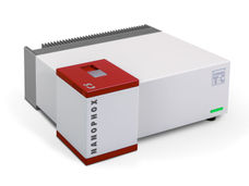
NANOPHOX CS by Sympatec
Particle size analysis in the nano range: Analyzing high concentrations with ease
Reliable results without time-consuming sample preparation
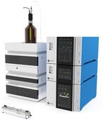
Eclipse by Wyatt Technology
FFF-MALS system for separation and characterization of macromolecules and nanoparticles
The latest and most innovative FFF system designed for highest usability, robustness and data quality

DynaPro Plate Reader III by Wyatt Technology
Screening of biopharmaceuticals and proteins with high-throughput dynamic light scattering (DLS)
Efficiently characterize your sample quality and stability from lead discovery to quality control
Get the chemical industry in your inbox
By submitting this form you agree that LUMITOS AG will send you the newsletter(s) selected above by email. Your data will not be passed on to third parties. Your data will be stored and processed in accordance with our data protection regulations. LUMITOS may contact you by email for the purpose of advertising or market and opinion surveys. You can revoke your consent at any time without giving reasons to LUMITOS AG, Ernst-Augustin-Str. 2, 12489 Berlin, Germany or by e-mail at revoke@lumitos.com with effect for the future. In addition, each email contains a link to unsubscribe from the corresponding newsletter.
