Mobile material analysis by NIR spectrometer in sugar cube format
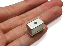
The Fraunhofer Institute for Photonic Microsystems IPMS will be presenting an extremely miniaturized near-infrared spectrometerThis device enables analysis of gaseous, liquid and solid materials immediately on site instead of taking samples for lab analysis. The optical bench is smaller than a sugar cube and thus it might fit into mobile devices as well as in automated process analysis tools.
Whether it is freshness testing of food, separation of plastics in recycling, analysis of raw materials in the pharmaceutical industry or measurements of the composition of liquids in automobile applications: in each case it is the time efficient qualitative and quantitative determination of the materials involved according to type and concentration. Spectroscopy, here the analysis of light scattered or attenuated by the material, is predestined for these types of applications. Measurements take place without direct contact and non-destructive to the samples.
Despite these advantages and while today’s market does offer many spectrometers for lab use there are few systems for simple on-location measurements. There are two major reasons for this: First most of these instruments use one or two dimensional photodiode arrays of III-V semiconductors like indium-gallium-arsenide, which inflate costs, and second they are voluminous for technological reasons. With miniaturized grating spectrometers this will change, says Dr. Heinrich Grüger, who is responsible for the »Sensors and Actuators Systems« business unit at Fraunhofer IPMS, where the spectrometer has been developed. »Our new hybrid-integrated system has a volume of 2.1 cm³ only, which is about 30% smaller than a common sugar cube. Due to its small outline and low power consumption of only a few milliwatts, it is ideal for integration into mobile measurement instruments and in situ measurements in facilities and buildings.«
With Fraunhofer IPMS scanning grating spectrometers, the light is diffracted on a movable optical grating realized in a MEMS technology. The device utilizes a resonantly driving principle of the grating which enables to scan a spectrum with a single highly sensitive detector instead of an array arrangement. The central element of the spectrometer is a MEMS chip which has been developed by Fraunhofer IPMS and measures just (9.5 × 5.3 × 0.5) mm³. The scientists realize this MEMS scanner featuring the diffraction grating and both optical slits directly on silicon wafers. A single 6″ silicon wafer is large enough for chips for hundreds of spectrometers on it. Applying hybrid-integration of the MEMS wafer with a spacer and an optical mirror substrate of identical size would mean that hundreds of spectrometers can be manufactured instantly. They are aligned and assembled and then separated into individual spectrometers. This means that the scientists don’t have to adjust the mirrors, gratings, slits and detectors piece by piece like required with conventional spectrometers. The advantage is clear: An enormous reduction in manufacturing costs. In addition, the MEMS based systems are distinctly more robust than conventional components manufactured with fine mechanics.
Other news from the department science
These products might interest you
Most read news
More news from our other portals
See the theme worlds for related content
Topic World Spectroscopy
Investigation with spectroscopy gives us unique insights into the composition and structure of materials. From UV-Vis spectroscopy to infrared and Raman spectroscopy to fluorescence and atomic absorption spectroscopy, spectroscopy offers us a wide range of analytical techniques to precisely characterize substances. Immerse yourself in the fascinating world of spectroscopy!
