X-rays show birth of semiconductor for blue LEDs
Gallium nitride is the second most important semiconductor material after silicon
Advertisement
Using a special pressure furnace, an international team of researchers has analysed the initial stages of the growth of the semiconductor gallium nitride with X-ray light. The observations show for the first time the atomic structure of the interface of the semiconductor material with liquid gallium under gentle growth conditions, as the team around Elias Vlieg from the Radboud University of Nijmegen in the Netherlands reports in the journal Physical Review Letters. The study is a first step towards a better understanding of the growth of this promising semiconductor material and to a better control of its growth.

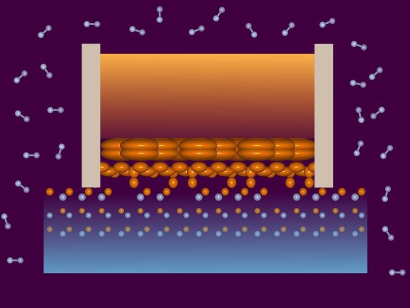
In the lower layers of the liquid gallium (centre), the atoms are located closer and closer to the horizontal position of the atoms in the crystal lattice (dots), as the X-ray investigation has shown. It also revealed surprisingly many defects in the upper layer of the crystal.
DESY, Vedran Vonk
“Gallium nitride is a mixture of the metal gallium and nitrogen, and is now the second most important semiconductor after silicon,” explains lead author Aryan de Jong, who wrote his doctoral thesis on this topic at Radboud University and is now working on gallium nitride applications in the semiconductor industry. “This is mainly due to blue light-emitting diodes, which cannot be produced on a silicon basis, but with gallium nitride.” In addition, gallium nitride is also interesting for other devices, as its larger band gap enables more stable devices, which is an advantage in harsh environments such as on satellites.
However, the production of suitable substrates, the so-called wafers, from gallium nitride is relatively complicated and costly. “For blue light-emitting diodes, the material is usually condensed from the gas phase. This is fairly easy to do, but the number of defects is relatively high, which is not so critical for light-emitting diodes, but for components such as microchips,” says Vedran Vonk from the DESY-Nanolab, the corresponding author of the publication. “What we are therefore looking for is an industrial process that allows gallium nitride to grow from a liquid with significantly fewer defects.”
Currently, this requires a pressure of several thousand atmospheres and high temperatures well above thousand degrees Celsius, which makes gallium nitride wafers expensive and severely limits their widespread application. However, what all liquid production processes have in common is the liquid-crystal interface which can already be examined at gentler conditions.
The researchers used a tailor-made pressurized furnace to examine the growth interface of a gallium nitride crystal with atomic precision using X-ray light. To this end, they placed a thin slice of a gallium nitride crystal in the furnace and placed a cylindrical container filled with liquid gallium on top, open at the bottom and sealed at the sides. Gallium already melts at about 30 degrees Celsius. The scientists filled the furnace with nitrogen up to 30 times atmospheric pressure and heated it to 850 degrees Celsius. “This does not yet correspond to the production conditions for large gallium nitride crystals, but it does provide insight into some of the basic processes involved in the growth of the crystal,” explains Vlieg.
The team used the X-ray light from the European Synchrotron Radiation Source ESRF in Grenoble (France) to examine the surface of the gallium nitride disk in the hot pressurized furnace. “The experiments revealed that the uppermost crystal layer had many more defects than expected – about every fourth gallium atom is missing in the crystal lattice,” reports Vonk. “They also showed that in the liquid gallium above the semiconductor crystal, layers form in which the gallium atoms of the liquid are located closer and closer to the gallium atoms of the crystal as they approach the boundary layer. This order and layering has never been observed before to this detail.”
The two unexpected observations improve our understanding of the growth of this promising semiconductor material and could help to discover a way to a simpler and more controllable production process. They also contribute to a better fundamental understanding of the processes at interfaces between liquid and solid phases of a metal.


