Flat gallium joins roster of new 2-D materials
Scientists introduce gallenene
Scientists at Rice University and the Indian Institute of Science, Bangalore, have discovered a method to make atomically flat gallium that shows promise for nanoscale electronics.
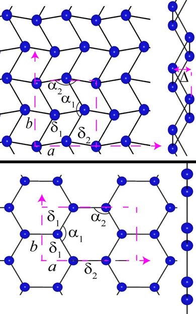
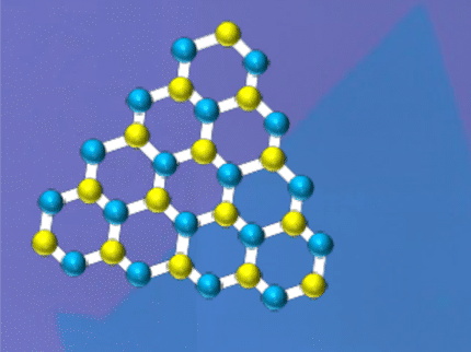
Models of the top and side structures of two forms of gallenene are shown after exfoliation from different sides of bulk gallium. Scientists at Rice University and the Indian Institute of Science, Bangalore, discovered a method to make atomically flat gallium that shows promise for nanoscale electronics.
Ajayan Research Group/Rice University
The Rice lab of materials scientist Pulickel Ajayan and colleagues in India created two-dimensional gallenene, a thin film of conductive material that is to gallium what graphene is to carbon.
Extracted into a two-dimensional form, the novel material appears to have an affinity for binding with semiconductors like silicon and could make an efficient metal contact in two-dimensional electronic devices, the researchers said.
Gallium is a metal with a low melting point; unlike graphene and many other 2-D structures, it cannot yet be grown with vapor phase deposition methods. Moreover, gallium also has a tendency to oxidize quickly. And while early samples of graphene were removed from graphite with adhesive tape, the bonds between gallium layers are too strong for such a simple approach.
So the Rice team led by co-authors Vidya Kochat, a former postdoctoral researcher at Rice, and Atanu Samanta, a student at the Indian Institute of Science, used heat instead of force.
Rather than a bottom-up approach, the researchers worked their way down from bulk gallium by heating it to 29.7 degrees Celsius (about 85 degrees Fahrenheit), just below the element's melting point. That was enough to drip gallium onto a glass slide. As a drop cooled just a bit, the researchers pressed a flat piece of silicon dioxide on top to lift just a few flat layers of gallenene.
They successfully exfoliated gallenene onto other substrates, including gallium nitride, gallium arsenide, silicone and nickel. That allowed them to confirm that particular gallenene-substrate combinations have different electronic properties and to suggest that these properties can be tuned for applications.
"The current work utilizes the weak interfaces of solids and liquids to separate thin 2-D sheets of gallium," said Chandra Sekhar Tiwary, principal investigator on the project he completed at Rice before becoming an assistant professor at the Indian Institute of Technology in Gandhinagar, India. "The same method can be explored for other metals and compounds with low melting points."
Gallenene's plasmonic and other properties are being investigated, according to Ajayan. "Near 2-D metals are difficult to extract, since these are mostly high-strength, nonlayered structures, so gallenene is an exception that could bridge the need for metals in the 2-D world," he said.
Original publication
Other news from the department science

Get the chemical industry in your inbox
By submitting this form you agree that LUMITOS AG will send you the newsletter(s) selected above by email. Your data will not be passed on to third parties. Your data will be stored and processed in accordance with our data protection regulations. LUMITOS may contact you by email for the purpose of advertising or market and opinion surveys. You can revoke your consent at any time without giving reasons to LUMITOS AG, Ernst-Augustin-Str. 2, 12489 Berlin, Germany or by e-mail at revoke@lumitos.com with effect for the future. In addition, each email contains a link to unsubscribe from the corresponding newsletter.
