NIST studies how new helium ion microscope measures up
Just as test pilots push planes to explore their limits, researchers at the National Institute of Standards and Technology (NIST) are probing the newest microscope technology to further improve measurement accuracy at the nanoscale. Better nanoscale measurements are critical for setting standards and improving production in the semiconductor and nanomanufacturing industries.
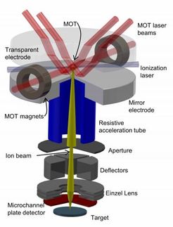
This new microscope technology uses helium ions to generate the signal used to image extremely small objects, a technique analogous to the scanning electron microscope, which was first introduced commercially in the 1960s. Paradoxically, although helium ions are far larger than electrons, they can provide higher resolution images with higher contrast. The depth of field is much better with the new technology too, so more of the image is in focus. “It is the physics,” explains Andras Vladar, SEM project leader in NIST’s Nanoscale-Metrology Group. “Ions have larger mass and shorter wavelength than electrons, so they can be better for imaging.” The images, he says, appear almost three-dimensional, revealing details smaller than a nanometer—the distance spanned by only three atoms in the silicon crystal.
NIST is working to understand the imaging mechanisms of this new technology. The clearest advantage of the helium ion microscope is that the images show the actual edge of a sample better than the SEM, which is critical in precision manufacturing. “Meeting critical dimensions by knowing where an edge is in high-tech manufacturing can mean the difference of hundreds of dollars per piece,” explains Michael Postek, chief of the NIST Precision Engineering Division and the nanomanufacturing program manager. Semiconductor manufacturers have multi-million dollar scanning electron microscopes all along their production lines to help control their microchip manufacturing processes.
“What we are learning,” explains Postek, “goes directly back to the manufacturers to improve their products, which allows NIST and industry to obtain the most precise measurements possible. We are transferring NIST technology and sharing our research with the semiconductor industry trade organization, SEMATECH.”
One such NIST contribution is “fast imaging,” a technique Vladar developed to obtain sharper images. A combination of vibrations at the nanoscale and taking images at high resolutions left certain images fuzzy, similar to what happens when taking a picture of a moving baby with a slow shutter speed. Instead of collecting the signal slowly and getting a fuzzy image, the NIST technique collects many images as fast as possible and merges them using a clever algorithm to reduce the fuzziness and result in a much sharper image.
Organizations
Other news from the department science
These products might interest you
Apreo 2 Scanning Electron Microscope by Thermo Fisher Scientific
Apreo 2 SEM: Scanning Electron Microscope with Impressive Resolution Specifications
Unmatched versatility powered by ChemiSEM Technology
JEOL SEM Series by JEOL
Scanning electron microscopy: Flexible systems for research and industry
From benchtop devices to FEG-SEM: customised solutions for precise analyses

Get the chemical industry in your inbox
By submitting this form you agree that LUMITOS AG will send you the newsletter(s) selected above by email. Your data will not be passed on to third parties. Your data will be stored and processed in accordance with our data protection regulations. LUMITOS may contact you by email for the purpose of advertising or market and opinion surveys. You can revoke your consent at any time without giving reasons to LUMITOS AG, Ernst-Augustin-Str. 2, 12489 Berlin, Germany or by e-mail at revoke@lumitos.com with effect for the future. In addition, each email contains a link to unsubscribe from the corresponding newsletter.
