New Clues to Mechanism for "Colossal Resistance" Effects
Understanding could lead to lower-power, increased-memory data-storage devices
Experiments at the U.S. Department of Energy's Brookhaven National Laboratory shed new light on some materials' ability to dramatically change their electrical resistance in the presence of an external magnetic or electric field. Small changes in resistance underlie many electronic devices, including some computer data storage systems. Understanding and applying dramatic resistance changes, known as colossal magnetoresistance, offers tremendous opportunities for the development of new technologies, including data-storage devices with increased data density and reduced power requirements. "This is an extremely important piece of work with broad potential application in developing the next generation of electronic and data-storage devices," said Brookhaven physicist Yimei Zhu, one of the lead authors on a paper appearing in Proceedings of the National Academy of Sciences. The Brookhaven scientists were studying crystalline perovskite manganites that had been doped with extra charge carriers - electrons or "holes" (the absence of electrons) - using various state-of-the-art electron microscopy techniques. In an unprecedented experiment, the scientists used a scanning-tunneling microscope that was built inside an electron microscope to apply an electric stimulus to the sample while observing its response at the atomic scale. Using this technique, the scientists obtained, for the first time, direct evidence that a small electric stimulus can distort the shape of the crystal lattice, and also cause changes in the way charges travel through the lattice. The lattice distortions accompanied the charge carrier as it moved through the lattice, producing a particle-like excitation called a polaron. "Polarons can be pictured as a charge carrier surrounded by a 'cloth' of the accompanying lattice vibrations," Zhu said. Zhu's group observed polarons melting and reordering - that is, undergoing a transition from solid to liquid to solid again - in response to the applied current, which the scientists have identified as the key mechanism for colossal mangetoresistance. The technique also allowed the scientists to study polaron behavior, i.e., how variations in electric field, current, and temperature affected this transition. "We show that static long-range ordering of polarons forms a polaron solid, which represents a new type of charge and orbital ordered state," said Zhu. "The related lattice distortions connect this phenomenon to colossal resistance effects, and suggest ways of modifying charge density and electronic interactions at the vicinity of electric interfaces and electrodes." Colossal resistance effects could result in miniaturization of electric circuits that operate at lower power. This work therefore has direct impact on the application of these materials in the development of new electronic and spintronic devices (devices that use 'a combination of electron spin and charge). Such devices include new forms of "nonvolatile" computer memory (memory that can retain stored information even when not powered) such as resistive random access memory (RRAM). This work was done in collaboration with Christian Jooss, a Brookhaven visiting scientist, and colleagues from the University of Goettingen, Germany. The work was funded by the Office of Basic Energy Sciences within the U.S. Department of Energy's Office of Science and by the German Research Foundation.

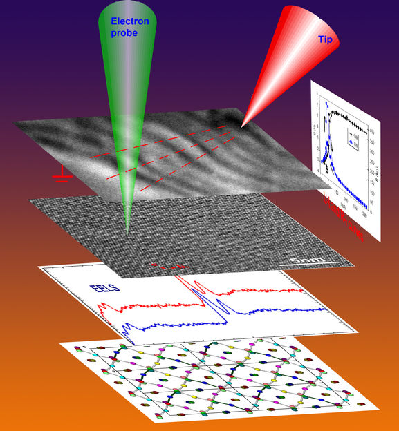
The method: Scientists used an electron probe (green) to make images and collect other data while using a scanning tunneling microscope tip (red) to apply current or an electric field to the sample. The first layered image of black lines shows polaron waves, which propagate during the application of the current. Fine dots in the second layer are the individual atoms, while the periodic dot-clusters show the electron ordered state. The graph of electron energy loss spectroscopy (EELS) reveals bonding-electron excitation. The bottom layer is a structural model of the crystal lattice. And the vertical graph shows the electric resistance (I-V curve) of the crystal when current is applied.
Brookhaven National Laboratory
Topics
Organizations
Other news from the department science

Get the chemical industry in your inbox
By submitting this form you agree that LUMITOS AG will send you the newsletter(s) selected above by email. Your data will not be passed on to third parties. Your data will be stored and processed in accordance with our data protection regulations. LUMITOS may contact you by email for the purpose of advertising or market and opinion surveys. You can revoke your consent at any time without giving reasons to LUMITOS AG, Ernst-Augustin-Str. 2, 12489 Berlin, Germany or by e-mail at revoke@lumitos.com with effect for the future. In addition, each email contains a link to unsubscribe from the corresponding newsletter.
Most read news
More news from our other portals
Last viewed contents

Scientists: a big step forward in the fight against nerve agents
BASF increases prices for pigments and dyes worldwide

Carbon nanostructure stronger than diamonds
Abgenix Completes Acquisition Of Immgenics
ZEISS Invests in UK Operations through Expansion of Cambridge Site
René_41


