Cryptographic potential in nanomaterial discovered
The ultimate defense against hackers may be just a few atoms thick
Advertisement
The next generation of electronic hardware security may be at hand as researchers at New York University Tandon School of engineering introduce a new class of unclonable cybersecurity security primitives made of a low-cost nanomaterial with the highest possible level of structural randomness. Randomness is highly desirable for constructing the security primitives that encrypt and thereby secure computer hardware and data physically, rather than by programming.

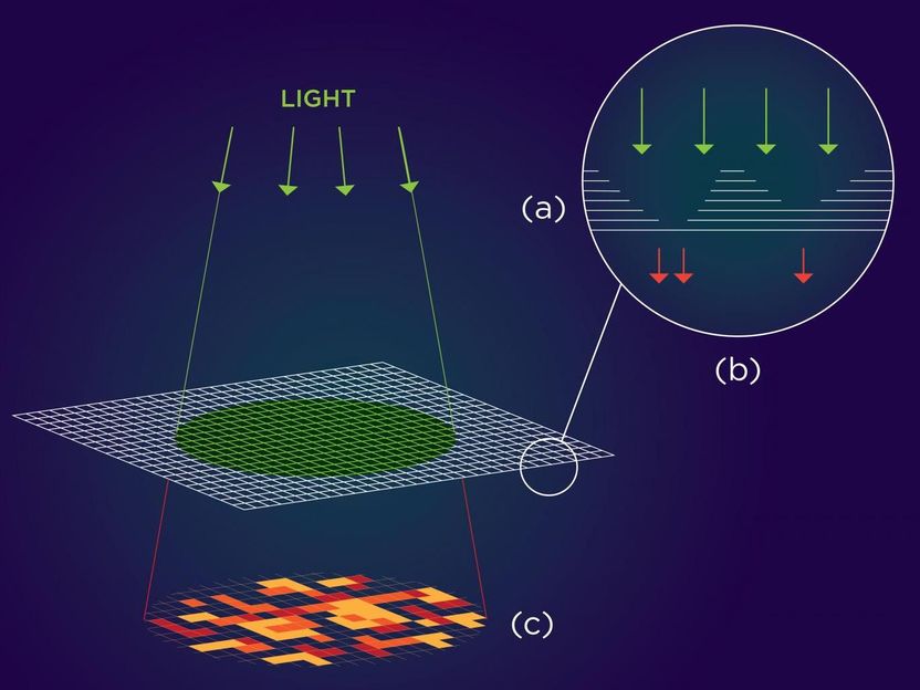
a) At monolayer thickness, this material has the optical properties of a semiconductor that emits light. At multilayer, the properties change and the material doesn't emit light. (b) Varying the thickness of each layer results in a thin film speckled with randomly occurring regions that alternately emit or block light. (c) Upon exposure to light, this pattern can be translated into a one-of-a-kind authentication key that could secure hardware components at minimal cost.
NYU Tandon: Althea Labre
Assistant Professor of Electrical and Computer Engineering Davood Shahrjerdi and his NYU Tandon team offer the first proof of complete spatial randomness in atomically thin molybdenum disulfide (MoS2). The researchers grew the nanomaterial in layers, each roughly one million times thinner than a human hair. By varying the thickness of each layer, Shahrjerdi explained, they tuned the size and type of energy band structure, which in turn affects the properties of the material.
"At monolayer thickness, this material has the optical properties of a semiconductor that emits light, but at multilayer, the properties change, and the material no longer emits light. This property is unique to this material," he said. By tuning the material growth process, the resulting thin film is speckled with randomly occurring regions that alternately emit or do not emit light. When exposed to light, this pattern translates into a one-of-a-kind authentication key that could secure hardware components at minimal cost.
Shahrjerdi said his team was pondering potential applications for what he described as the beautiful random light patterns of MoS2 when he realized it would be highly valuable as a cryptographic primitive.
This represents the first physically unclonable security primitive created using this nanomaterial. Typically embedded in integrated circuits, physically unclonable security primitives protect or authenticate hardware or digital information. They interact with a stimulus -- in this case, light -- to produce a unique response that can serve as a cryptographic key or means of authentication.
The research team envisions a future in which similar nanomaterial-based security primitives can be inexpensively produced at scale and applied to a chip or other hardware component, much like a postage stamp to a letter. "No metal contacts are required, and production could take place independently of the chip fabrication process," Shahrjerdi said. "It's maximum security with minimal investment."


