Factors in the fabrication of heterojunctions of 2D-materials through CVD
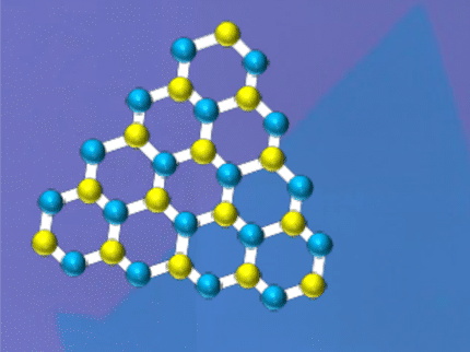
2D-materials have special lattice structures. Atoms in the same layer were usually bound by the covalent bond, while the force between layers is van der Waals coupling. They have super clean surfaces without any dangling bonds. Thus, the design of heterojunctions will be flexible when 2D-materials are utilized to constitute heterojunctions. The heterojunctions formed by different 2D-materials have advantageous properties compared with their corresponding single-component 2D-material, such as optimizing band alignment, bandgap, charge transfer and optical properties. The research of heterojunctions is a hot topic in 2D-material field.

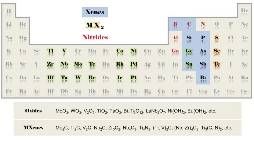
This figure shows the distribution of elements of different 2-D materials.
©Science China Press
In a review article, the methods of chemical vapor deposition (CVD) to fabricate 2D heterojunctions are referred based on researches in the last few years. Firstly, the development history of heterojunctions of 2D-materials is introduced. And then, the influences of different growth conditions on heterojunctions are discussed. Finally, some other methods to prepare heterojunctions are referred.
The transfer method is a convenience good technique for heterojunctions of 2D-materials in labs. Researchers can easily utilize this method to obtain the specific heterojunction they want. But it is not enough for the extensive applications, an efficient and stable technique is necessary. The chemical vapor deposition is introduced to fabricate heterojunctions as a potential method. The chemical vapor deposition method is sensitive to the changes of growth conditions. It is an important research topic to ascertain influences of different factors on the growth process and final heterojunctions. This review classifies the factors into temperature, substrate, precursor, lattice mismatch, carrier gas flow rate, and carrier gas composition. When anyone of factors is changed, the obtained heterojunctions will have different structures or components. These factors also influence each other. So, the desired heterojunctions of 2D-materials can't be fabricated by just modifying one parameter of the chemical vapor deposition system. For example, when different precursors are used, the growth temperature should be reset due to the different evaporating temperatures of different precursors. Besides these, the method through sulfuring patterned films, such as metal films, oxide films and other component films, to fabricate heterojunctions is also referred.
The further researches are necessary to solve problems in the fabrication of heterojunctions of 2D-materials. MBE and MOCVD can also be considered as good options of the fabrication technique.
Original publication
Cui Yu Li Bo LI Jingbo Wei Zhongming; "Chemical Vapor Deposition Growth of Two-dimensional Heterojunctions"; Physics, Mechanics & Astronomy; 2017
Most read news
Original publication
Cui Yu Li Bo LI Jingbo Wei Zhongming; "Chemical Vapor Deposition Growth of Two-dimensional Heterojunctions"; Physics, Mechanics & Astronomy; 2017
Topics
Organizations
Other news from the department science

Get the chemical industry in your inbox
By submitting this form you agree that LUMITOS AG will send you the newsletter(s) selected above by email. Your data will not be passed on to third parties. Your data will be stored and processed in accordance with our data protection regulations. LUMITOS may contact you by email for the purpose of advertising or market and opinion surveys. You can revoke your consent at any time without giving reasons to LUMITOS AG, Ernst-Augustin-Str. 2, 12489 Berlin, Germany or by e-mail at revoke@lumitos.com with effect for the future. In addition, each email contains a link to unsubscribe from the corresponding newsletter.


