Semiconductor dynamics may help improve energy efficiency
Researchers examining the flow of electricity through semiconductors have uncovered another reason these materials seem to lose their ability to carry a charge as they become more densely "doped." Their results may help engineers design faster semiconductors in the future.
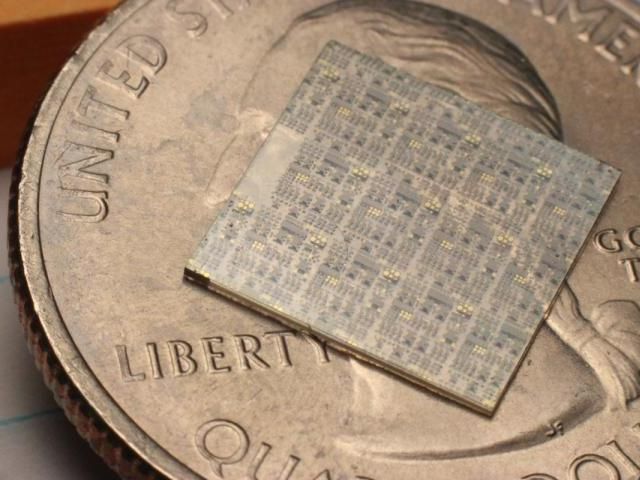
Semiconductors are found in just about every piece of modern electronics, from computers to televisions to your cell phone. They fall somewhere between metals, which conduct electricity very well, and insulators like glass that don't conduct electricity at all. This moderate conduction property is what allows semiconductors to perform as switches and transistors in electronics.
The most common material for semiconductors is silicon, which is mined from the earth and then refined and purified. But pure silicon doesn't conduct electricity, so the material is purposely and precisely adulterated by the addition of other substances known as dopants. Boron and phosphorus ions are common dopants added to silicon-based semiconductors that allow them to conduct electricity.
But the amount of dopant added to a semiconductor matters - too little dopant and the semiconductor won't be able to conduct electricity. Too much dopant and the semiconductor becomes more like a non-conductive insulator.
"There's a sweet spot when it comes to doping where the right amount allows for the efficient conduction of electricity, but after a certain point, adding more dopants slows down the flow," says Preston Snee, associate professor of chemistry at the University of Illinois at Chicago and corresponding author on the paper.
"For a long time scientists thought that the reason efficient conduction of electricity dropped off with the addition of more dopants was because these dopants caused the flowing electrons to be deflected away, but we found that there's also another way too many dopants impede the flow of electricity."
Snee, UIC chemistry student Asra Hassan, and their colleagues wanted to get a closer look at what happens when electricity flows through a semiconductor.
Using the Advanced Photon Source Argonne National Laboratory, they were able to capture X-ray images of what happens at the atomic level inside a semiconductor. They used tiny chips of cadmium sulfide for their semiconductor "base" and doped them with copper ions. Instead of wiring the tiny chips for electricity, they generated a flow of electrons through the semiconductors by shooting them with a powerful blue laser beam. At the same time, they took very high energy X-ray photos of the semiconductors at millionths of a microsecond apart - which showed what was happening at the atomic level in real time as electrons flowed through the doped semiconductors.
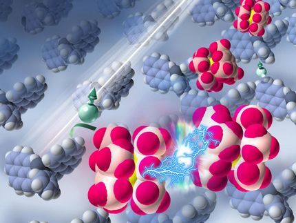
They found that when electrons were flowing through, the copper ions transiently formed bonds with the cadmium sulfate semiconductor base, which is detrimental to conduction.
"This has never been seen before," said Hassan. "Electrons are still bouncing off dopants, which we knew already, but we now know of this other process that contributes to impeding flow of electricity in over-doped semiconductors."
The bonding of the dopant ions to the semiconductor base material "causes the current to get stuck at the dopants, which we don't want in our electronics, especially if we want them to be fast and efficient," she said. "However, now that we know this is happening inside the material, we can design smarter systems that minimize this effect, which we call 'charge carrier modulation of dopant bonding'."
Original publication
Asra Hassan, Xiaoyi Zhang, Xiaohan Liu, Clare E. Rowland, Ali M. Jawaid, Soma Chattopadhyay, Ahmet Gulec, Armen Shamirian, Xiaobing Zuo, Robert F. Klie, Richard D. Schaller, and Preston T. Snee; "Charge Carriers Modulate the Bonding of Semiconductor Nanoparticle Dopants As Revealed by Time-Resolved X-ray Spectroscopy"; ACS Nano; 2017
Topics
Organizations
Other news from the department science

Get the chemical industry in your inbox
By submitting this form you agree that LUMITOS AG will send you the newsletter(s) selected above by email. Your data will not be passed on to third parties. Your data will be stored and processed in accordance with our data protection regulations. LUMITOS may contact you by email for the purpose of advertising or market and opinion surveys. You can revoke your consent at any time without giving reasons to LUMITOS AG, Ernst-Augustin-Str. 2, 12489 Berlin, Germany or by e-mail at revoke@lumitos.com with effect for the future. In addition, each email contains a link to unsubscribe from the corresponding newsletter.
Most read news
More news from our other portals
Last viewed contents
Clariant doubles capacity for pigments and pigment preparations in India - Expansion represents an investment in production facilities
BASF and SINOPEC consider further expansion of Nanjing joint venture
Category:Dielectrics
Sinochem Ranked as "China's Most Influential Enterprises"
Motherwort
Scientists capture colliding organic nanoparticles on video for first time
BASF and Sinopec complete second phase of Nanjing investment, announce new plans for expansion - New acrylic acid plant to be established
GPC Biotech announces two milestones in expanded anti-microbial alliance with Altana Subsidiary Byk Gulden
ASTM International Declarable Substances Committee Approves First Test Method

BASF Group: Strong performance in Q4 2020 due to higher volumes and prices - Bonus for employees as a sign of recognition and appreciation

MIRA P Basic | Raman spectrometers | Metrohm


