2-D material's traits could send electronics R&D spinning in new directions
An international team of researchers, working at the Department of Energy's Lawrence Berkeley National Laboratory (Berkeley Lab) and UC Berkeley, fabricated an atomically thin material and measured its exotic and durable properties that make it a promising candidate for a budding branch of electronics known as "spintronics."

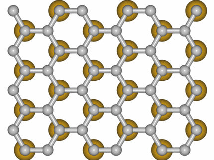
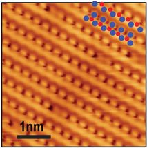
This is a scanning tunneling microscopy image of a 2-D material created and studied at Berkeley Lab's Advanced Light Source (orange, background). In the upper right corner, the blue dots represent the layout of tungsten atoms and the red dots represent tellurium atoms.
Berkeley Lab
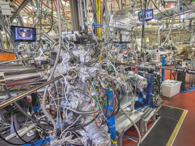
Beamline 10.0.1 at Berkeley Lab's Advanced Light Source enables researchers to both create and study the properties of atomically thin materials.
Roy Kaltschmidt/Berkeley Lab

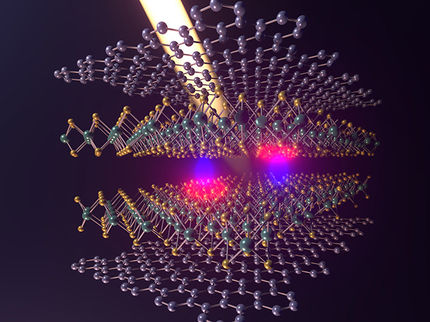
The material - known as 1T'-WTe2 - bridges two flourishing fields of research: that of so-called 2-D materials, which include monolayer materials such as graphene that behave in different ways than their thicker forms; and topological materials, in which electrons can zip around in predictable ways with next to no resistance and regardless of defects that would ordinarily impede their movement.
At the edges of this material, the spin of electrons - a particle property that functions a bit like a compass needle pointing either north or south - and their momentum are closely tied and predictable.
This latest experimental evidence could elevate the material's use as a test subject for next-gen applications, such as a new breed of electronic devices that manipulate its spin property to carry and store data more efficiently than present-day devices. These traits are fundamental to spintronics.
The material is called a topological insulator because its interior surface does not conduct electricity, and its electrical conductivity (the flow of electrons) is restricted to its edges.
"This material should be very useful for spintronics studies," said Sung-Kwan Mo, a physicist and staff scientist at Berkeley Lab's Advanced Light Source (ALS) who co-led the study.
"The flow of electrons is completely linked with the direction of their spins, and is limited only to the edges of the material," Mo said. "The electrons will travel in one direction, and with one type of spin, which is a useful quality for spintronics devices." Such devices could conceivably carry data more fluidly, with lesser power demands and heat buildup than is typical for present-day electronic devices.
"We're excited about the fact that we have found another family of materials where we can both explore the physics of 2-D topological insulators and do experiments that may lead to future applications," said Zhi-Xun Shen, a professor in Physical Sciences at Stanford University and the Advisor for Science and Technology at SLAC National Accelerator Laboratory who also co-led the research effort. "This general class of materials is known to be robust and to hold up well under various experimental conditions, and these qualities should allow the field to develop faster," he added.
The material was fabricated and studied at the ALS, an X-ray research facility known as a synchrotron. Shujie Tang, a visiting postdoctoral researcher at Berkeley Lab and Stanford University, and a co-lead author in the study, was instrumental in growing 3-atom-thick crystalline samples of the material in a highly purified, vacuum-sealed compartment at the ALS, using a process known as molecular beam epitaxy.
The high-purity samples were then studied at the ALS using a technique known as ARPES (or angle-resolved photoemission spectroscopy), which provides a powerful probe of materials' electron properties.
"After we refined the growth recipe, we measured it with ARPES. We immediately recognized the characteristic electronic structure of a 2-D topological insulator," Tang said, based on theory and predictions. "We were the first ones to perform this type of measurement on this material."
But because the conducting part of this material, at its outermost edge, measured only a few nanometers thin - thousands of times thinner than the X-ray beam's focus - it was difficult to positively identify all of the material's electronic properties.
So collaborators at UC Berkeley performed additional measurements at the atomic scale using a technique known as STM, or scanning tunneling microscopy. "STM measured its edge state directly, so that was a really key contribution," Tang said.
The research effort, which began in 2015, involved more than two dozen researchers in a variety of disciplines. The research team also benefited from computational work at Berkeley Lab's National Energy Research Scientific Computing Center (NERSC).
Two-dimensional materials have unique electronic properties that are considered key to adapting them for spintronics applications, and there is a very active worldwide R&D effort focused on tailoring these materials for specific uses by selectively stacking different types.
"Researchers are trying to sandwich them on top of each other to tweak the material as they wish - like Lego blocks," Mo said. "Now that we have experimental proof of this material's properties, we want to stack it up with other materials to see how these properties change."
A typical problem in creating such designer materials from atomically thin layers is that materials typically have nanoscale defects that can be difficult to eliminate and that can affect their performance. But because 1T'-WTe2 is a topological insulator, its electronic properties are by nature resilient.
"At the nanoscale it may not be a perfect crystal," Mo said, "but the beauty of topological materials is that even when you have less than perfect crystals, the edge states survive. The imperfections don't break the key properties."
Going forward, researchers aim to develop larger samples of the material and to discover how to selectively tune and accentuate specific properties. Besides its topological properties, its "sister materials," which have similar properties and were also studied by the research team, are known to be light-sensitive and have useful properties for solar cells and for optoelectronics, which control light for use in electronic devices.
Original publication
Other news from the department science
Most read news
More news from our other portals
See the theme worlds for related content
Topic World Spectroscopy
Investigation with spectroscopy gives us unique insights into the composition and structure of materials. From UV-Vis spectroscopy to infrared and Raman spectroscopy to fluorescence and atomic absorption spectroscopy, spectroscopy offers us a wide range of analytical techniques to precisely characterize substances. Immerse yourself in the fascinating world of spectroscopy!
