Electrostatic design of materials: A fundamentally new approach
Collective electrostatic effects are used to intentionally manipulate material properties
Advertisement
Computational materials design is traditionally used to improve and further develop already existing materials. Simulations grant a deep insight into the quantum mechanical effects which determine material properties. Egbert Zojer and his team at the Institute of Solid State Physics of TU Graz go a decisive step beyond that: they use computer simulations to propose an entirely new concept for controlling the electronic properties of materials. Potentially disturbing influences arising from the regular arrangement of polar elements, so-called collective electrostatic effects, are used by the research group to intentionally manipulate material properties. That this radically new approach also works for three-dimensional materials has been demonstrated by the Graz team.

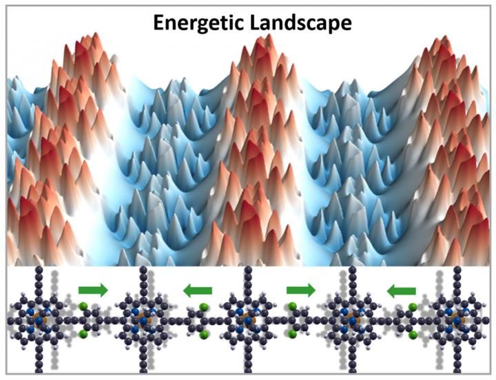
This image shows 3-D vision of the manipulated energy landscape within 3-D bulk material.
© TU Graz
Manipulation of the energetic materials landscape
"The basic approach of the electrostatic design concept is to modify the electronic states of semiconductors via the periodic arrangement of dipolar groups. In this way we are able to locally manipulate energy levels in a controlled way. In doing so, we do not try to find ways to bypass such effects which are inevitable especially at interfaces. Rather, we make deliberate use of them for our own purposes," explains Egbert Zojer.
This topic has been in the focus of the research of the Zojer group already for some time. The first step was the electrostatic design of molecular monolayers, for example on gold electrodes. Experiments have shown that the predicted energy shifts within the layers actually take place and that charge transport through monolayers can be deliberately modulated. Also, the electronic states of two-dimensional materials, such as graphene, can be controlled by means of collective electrostatic effects. Doctoral student Veronika Obersteiner, Egbert Zojer and other colleagues from the team demonstrate the full potential of the concept by extending it to three-dimensional materials.
"For the example of three-dimensional covalent organic networks, we show how - by means of collective electrostatic effects - the energy landscape within three-dimensional bulk material can be manipulated such that spatially confined pathways for electrons and holes can be realised. In this way charge carriers can, for instance, be separated and the electronic properties of the material can be designed as desired," says Zojer.
The concept is especially interesting for solar cells. In classical organic solar cells, chemically different building blocks, so-called donors and acceptors, are used to separate the photogenerated electron-hole pairs. In the approach proposed here, the necessary local shift of energy levels occurs due to the periodic arrangement of polar groups. The semiconducting areas onto which the electrons and holes are shifted are chemically identical. "In this way, we can quasi-continuously and efficiently fine tune the energy levels by varying the dipole density. This work is the climax to our intensive research on the electrostatic design of materials," says Zojer.
Electrostatic design in 3D systems can also enable the realization of complex quantum structures, such as quantum-cascades and quantum-checkerboards. "Only the imagination of the materials designer can set limits to our concept," Zojer and Obersteiner enthuse in unison.
Computational operations for this paper had been executed at the Vienna Scientific Cluster (VSC), Austria's highest performing supercomputer and a joint operation of the partner universities TU Wien, TU Graz, University of Vienna, Boku Vienna and University of Innsbruck. This work is anchored in the Field of Expertise "Advanced Materials Science", one of five research foci of TU Graz.


