Shipley Company Develops New Copper Plating Chemistry for 300mm Wafers
Shipley Company, L.L.C., a world leader of innovative electronic materials and technology, has recently developed a new three-component copper plating chemical system for advanced interconnect applications. The benefits of the copper plating chemistry include: robust gapfill, ultra-level copper film deposition (small and large features), uniform high- and low-aspect-ratio plating of sub-150 nm vias and trench structures and is easily integrated into associated interconnect fabrication processes. The newly developed organic additives in combination with the corresponding Shipley copper electrolyte, are ideally suited for the most challenging plating applications. Shipley has also developed analytical standards (system calibration and process control materials) for precise and accurate control of the plating bath during production plating. Results with the new plating chemistry will be featured at the Shipley Far East booth, 8-A601, during the Semicon Japan trade show held on December 5-7, 2002, at the Makuhari Messe (Nippon Convention Center), Tokyo, Japan.
The Shipley three-component system is the result of a long-term research effort designed to understand the fundamentals of copper electroplating. Shipley research personnel located at the company's corporate research facility, Marlborough, MA, U.S.A, have developed a clear understanding of the multi-component interactions in an electroplating bath during the electro-chemical plating process. These insights will serve as an accurate predictor of copper plating by-product formation and concentration. Novel molecules were individually selected for their contribution to the system. A close technology-sharing relationship with each of the top plating system manufacturers has accelerated product development efforts at Shipley, resulting in optimized plating performance with their tools.
The new Shipley plating chemistry meets the technical requirements for plating 300 mm wafers at the 65 nm technology node while delivering superior plating bath lifetime characteristics. Additionally, it has shown to deliver a highly reflective copper deposit with very low surface roughness, thereby minimizing defects.
Most read news
Other news from the department research and development
These products might interest you

Certified reference materials of the European Commission's Joint Research Centre by ERM
Certified reference materials for the analysis of environmental,food,clinical and industrial samples
Certified reference materials (CRMs) provide confidence in the correctness of analytical results
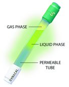
Permeation Devices by VICI
Create Your Own Calibration Gas Standards
Permeation Devices vs. Bottled Trace Level Standards
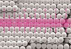
NanoStandard™ / MicroStandard™ by Applied Microspheres
Highly uniform polymer particle size standards, with traceable mean diameters
Traceable both to the international System of Units (SI) and NIST

Get the chemical industry in your inbox
By submitting this form you agree that LUMITOS AG will send you the newsletter(s) selected above by email. Your data will not be passed on to third parties. Your data will be stored and processed in accordance with our data protection regulations. LUMITOS may contact you by email for the purpose of advertising or market and opinion surveys. You can revoke your consent at any time without giving reasons to LUMITOS AG, Ernst-Augustin-Str. 2, 12489 Berlin, Germany or by e-mail at revoke@lumitos.com with effect for the future. In addition, each email contains a link to unsubscribe from the corresponding newsletter.
