Nanocavity and atomically thin materials advance tech for chip-scale light sources
When an individual uses Facebook or searches Google, the information processing happens in a large data center. Short distance optical interconnects can improve the performance of these data centers. Current systems utilize electrons, which could cause overheating and wastes power. However, utilizing light to transfer information between computer chips and boards can improve efficiency.
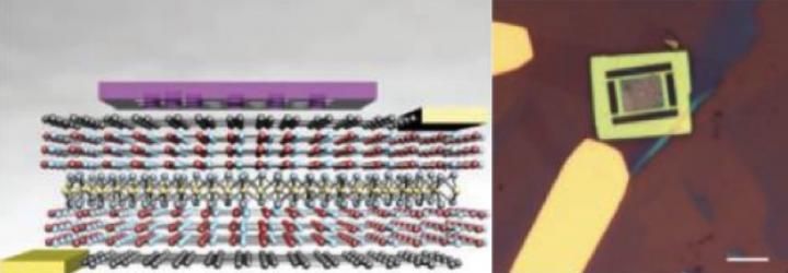
Figure 1 shows the schematic of the 2-D material heterostructure on top of which the photonic crystal cavity is transferred. Figure 2 shows the optical microscope image of the cavity transferred on the 2-D material heterostructure.
University of Washington
University of Washington Assistant Professor of Electrical Engineering and Physics Arka Majumdar, Associate Professor of Materials Science and Engineering and Physics Xiaodong Xu and their team have discovered an important first step towards building electrically pumped nanolasers (or light-based sources). These lasers are critical in the development of integrated photonic based short-distance optical interconnects and sensors.
The team demonstrated this first step through cavity-enhanced electroluminescence from atomically thin monolayer materials. The thinness of this material yields efficient coordination between the two key components of the laser. Both the cavity-enhanced electroluminescence and material will allow energy-efficient data centers and support high performance parallel computing.
Recently discovered atomically thin semiconductors have generated significant interest due to showing light emission in the 2D limit. However, due to the extreme thinness of this material, its emission intensity is usually not strong enough, and it is important to integrate them with photonic devices (nano-lasers, in this case) to get more light out.
"Researchers have demonstrated electroluminescence in this material [atomically thin monolayer]," Majumdar said. "Last year, we also reported the operation of an ultra-low threshold optically pumped laser, using this material integrated with nano-cavity. But for practical applications, electrically driven devices are required. Using this, one can power the devices using electrical current. For example, you power your laser pointer using an electrical battery. "
Majumdar and Xu recently reported cavity-enhanced electroluminescence in atomically thin material. A heterostructure of different monolayer materials are used to enhance the emission. Without the cavity, the emission is broadband (unidirectional) and weak. A nano-cavity enhances the emission and also enables single-mode (directed) operation. This allows direct modulation of the emission, a crucial requirement for the data-communication.
These structures are of current scientific interest and are considered the new "gold rush" of condensed matter physics and materials science. Their current result and the previous demonstration of optically pumped lasers show the promise of electrically pumped nano-lasers, which constitutes the next milestone for this research. This next achievement will improve data center efficiency for optimal performance.
"Our team is currently exploring integration of the monolayer materials with a silicon nitride platform," Majumdar said. "Through this work, we hope to achieve the coveted CMOS [complementary metal-oxide-semiconductor] compatibility, which is the same process by which the computer processors are fabricated today."
Original publication
Other news from the department science

Get the chemical industry in your inbox
By submitting this form you agree that LUMITOS AG will send you the newsletter(s) selected above by email. Your data will not be passed on to third parties. Your data will be stored and processed in accordance with our data protection regulations. LUMITOS may contact you by email for the purpose of advertising or market and opinion surveys. You can revoke your consent at any time without giving reasons to LUMITOS AG, Ernst-Augustin-Str. 2, 12489 Berlin, Germany or by e-mail at revoke@lumitos.com with effect for the future. In addition, each email contains a link to unsubscribe from the corresponding newsletter.
Most read news
More news from our other portals
Last viewed contents
Lespedeza
Structure formation during freeze casting filmed in 3D and real time - Freeze-cast materials can be used for many applications: as battery electrodes, catalyst materials or in biomedicine
WACKER Officially Opens US-based R&D Center for Silicones in Ann Arbor, MI
Princess_cut
Townsend_coefficient
High-resolution atomic imaging of specimens in liquid by TEM using graphene liquid cell - Looking into specimens on an atomic level in liquids, and understanding atomic processes so far regarded impossible
