Lighting up ultrathin films
Advertisement
Based on a study of the optical properties of novel ultrathin semiconductors, researchers of Ludwig-Maximilians-Universitaet (LMU) in Munich have developed a method for rapid and efficient characterization of these materials.

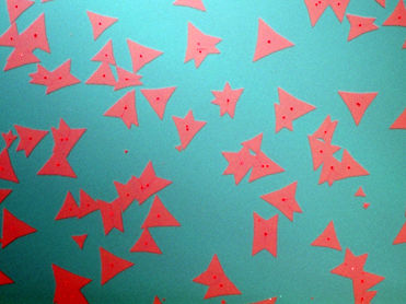
Light micrograph showing two-dimensional crystals of the thin-film semiconductor molybdenum disulfide
Hisato Yamaguchi (Los Alamos National Laboratory, USA)
Chemical compounds based on elements that belong to the so-called transition metals can be processed to yield atomically thin two-dimensional crystals consisting of a monolayer of the composite in question. The resulting materials are semiconductors with surprising optical properties. In cooperation with American colleagues, a team of LMU physicists led by Alexander Högele has now explored the properties of thin-film semiconductors made up of transition metal dichalcogenides (TMDs).
These semiconductors exhibit remarkably strong interaction with light and therefore have great potential for applications in the field of opto-electronics. In particular, the electrons in these materials can be excited with polarized light. "Circularly polarized light generates charge carriers that exhibit either left- or right-handed circular motion. The associated angular momentum is quantized and described by the so-called valley index which can be detected as valley polarization," Högele explains. In accord with the laws of quantum mechanics, the valley index can be used just like quantum mechanical spin to encode information for many applications including quantum computing.
However, recent studies of the valley index in TMD semiconductors have led to controversial results. Different groups worldwide have reported inconsistent values for the degree of valley polarization. With the aid of their newly developed polarimetric method and using monolayers of the semiconducting TMD molybdenum disulfide as a model system, the LMU researchers have now clarified the reasons for these discrepancies: "Response to polarized light turns out to be very sensitive to the quality of the crystals, and can thus vary significantly within the same crystal," Högele says. "The interplay between crystal quality and valley polarization will allow us to measure rapidly and efficiently those properties of the sample that are relevant for applications based on the valley quantum degree of freedom."
Moreover, the new method can be applied to other monolayer semiconductors and systems made up of several different materials. In the future, this will enable the functionalities of devices based on atomically thin semiconductors -- such as novel types of LEDs -- to be characterized swiftly and economically.


