GaN-on-Silicon for scalable high electron mobility transistors
A team of researchers at the University of Illinois at Urbana-Champaign has advanced gallium nitride (GaN)-on-silicon transistor technology by optimizing the composition of the semiconductor layers that make up the device. Working with industry partners Veeco and IBM, the team created the high electron mobility transistor (HEMT) structure on a 200 mm silicon substrate with a process that will scale to larger industry-standard wafer sizes.
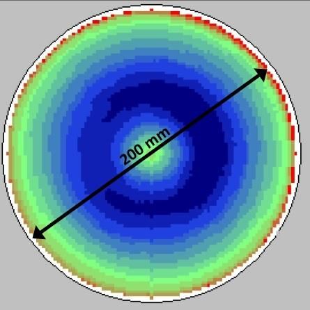
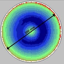
This is a GaN on 200 mm Si wafer thickness mapping image.
University of Illinois
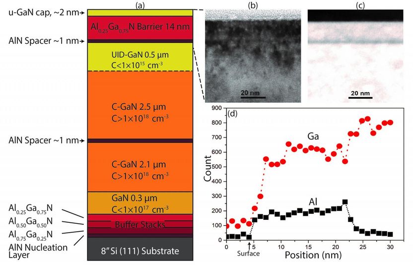
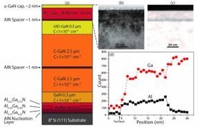
a) Cross sectional structure. b) TEM image of top 80 nm of the HEMT structure. The dark gray layer marks the start of the surface. c) STEM image of top 80 nm. The surface starts beneath the black layer and the dark band in the image is the AlN spacer. d) EDS Chemical Analysis of top 25 nm. Data before 4 nm are the background values from above the surface.
University of Illinois
Can Bayram, an assistant professor of electrical and computer engineering (ECE), and his team have created the GaN HEMT structure on a silicon platform because it is compatible with existing CMOS manufacturing processes and is less expensive than other substrate options like sapphire and silicon carbide.
However, silicon does have its challenges. Namely, the lattice constant, or space between silicon atoms, doesn't match up with the atomic structure of the GaN grown on top of it.
"When you grow the GaN on top, there's a lot of strain between the layers, so we grew buffer layers [between the silicon and GaN] to help change the lattice constant into the proper size," explained ECE undergraduate researcher Josh Perozek.
Without these buffer layers, cracks or other defects will form in the GaN material, which would prevent the transistor from operating properly. Specifically, these defects -- threading dislocations or holes where atoms should be--ruin the properties of the 2-dimensional electron gas channel in the device. This channel is critical to the HEMTs ability to conduct current and function at high frequencies.
"The single most important thing for these GaN [HEMT] devices is to have high 2D electron gas concentration," said Bayram, about the accumulation of electrons in a channel at the interface between the silicon and the various GaN-based layers above it.
"The problem is you have to control the strain balance among all those layers--from substrate all the way up to the channel -- so as to maximize the density of the of the conducting electrons in order to get the fastest transistor with the highest possible power density."
After studying three different buffer layer configurations, Bayram's team discovered that thicker buffer layers made of graded AlGaN reduce threading dislocation, and stacking those layers reduces stress. With this type of configuration, the team achieved an electron mobility of 1,800 cm2/V-sec.
"The less strain there is on the GaN layer, the higher the mobility will be, which ultimately corresponds to higher transistor operating frequencies," said Hsuan-Ping Lee, an ECE graduate student researcher leading the scaling of these devices for 5G applications.
According to Bayram, the next step for his team is to fabricate fully functional high-frequency GaN HEMTs on a silicon platform for use in the 5G wireless data networks.
When it's fully deployed, the 5G network will enable faster data rates for the world's 8 billion mobile phones, and will provide better connectivity and performance for Internet of Things (IoT) devices and driverless cars.
Original publication
Original publication
J Perozek, H-P Lee, B Krishnan, A Paranjpe, K B Reuter, D K Sadana and C Bayram; Investigation of structural, optical, and electrical characteristics of an AlGaN/GaN high electron mobility transistor structure across a 200 mm Si(1 1 1) substrate"; Journal of Physics D: Applied Physics; 2017
Topics
Organizations
Other news from the department science

Get the chemical industry in your inbox
By submitting this form you agree that LUMITOS AG will send you the newsletter(s) selected above by email. Your data will not be passed on to third parties. Your data will be stored and processed in accordance with our data protection regulations. LUMITOS may contact you by email for the purpose of advertising or market and opinion surveys. You can revoke your consent at any time without giving reasons to LUMITOS AG, Ernst-Augustin-Str. 2, 12489 Berlin, Germany or by e-mail at revoke@lumitos.com with effect for the future. In addition, each email contains a link to unsubscribe from the corresponding newsletter.
Most read news
More news from our other portals
Last viewed contents
Open_hearth_furnace

Maize and milk proteins can replace fossil fuels and metals in the production of nanostructured surfaces - Sustainably produced nanotechnology
Activin
TGF_beta
Basell launches new Metocene metallocene-based polypropylene grade targeted to customer TWIM
Eindhoven researchers observe shell growth thanks to 'ion sponge' - Revolutionary microscope technology confirms 30-year-old theory
Pfizer Acted Responsibly In Sharing Celebrex Alzheimer's Study Data With FDA - Public Citizen Charge is Misleading and Unfair to Patients
R&D for Next-Generation Solid State Batteries - Partnership between Fraunhofer and Hydro-Québec

Engineers develop 'chameleon metals' that change surfaces in response to heat
Hitachi selects Agilent Technologies' microarrays for pharmaceutical research
Operation_Antler_(Porton_Down_investigation)


