Random Access Memory on a Low Energy Diet
Researchers develop basis for a novel memory chip
Memory chips are among the most basic components in computers. The random access memory is where processors temporarily store their data, which is a crucial function. Researchers from Dresden and Basel have now managed to lay the foundation for a new memory chip concept. It has the potential to use considerably less energy than the chips produced to date – this is important not only for mobile applications but also for big data computing centers.
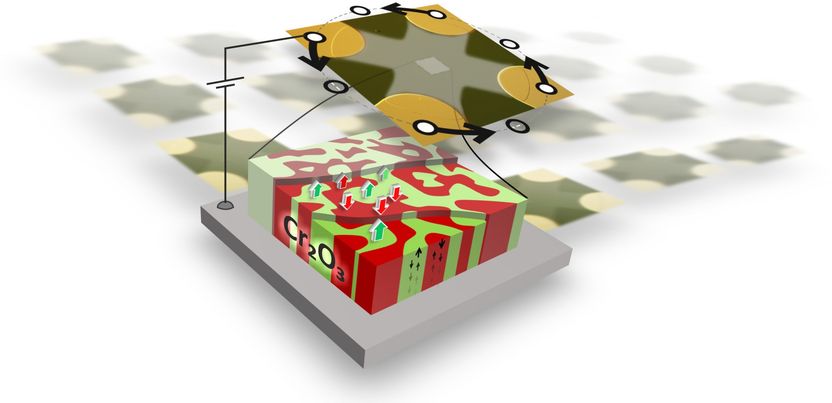
The prototype of an antiferromagnetic magnetoelectric memory chip, which was invented by researchers from Dresden and Basel. It consists of a thin layer of chromium oxide (Cr2O3) for saving data, on top of which the physicists attached a nanometer-thin platinum layer for read out.
T. Kosub
The purely electrical memory chips that are commonly used today have a significant disadvantage: “This memory is volatile and its state must be continuously refreshed,” says Dr. Tobias Kosub, first author of the study and post-doctoral researcher at the Helmholtz-Zentrum Dresden-Rossendorf (HZDR). “This requires quite a lot of energy.” The consequences can be seen, for example, at large computing centers. On the one hand, their electricity bills rise with increased computing power. On the other hand, the chips increasingly heat up based on their energy consumption. The data centers are finding it increasingly difficult to dissipate this heat. Some Cloud operators go as far as to set up their server farms in cold regions.
There is an alternative to these electrical memory chips. MRAMs save data magnetically and therefore do not require constant refreshing. They do, however, require relatively large electrical currents to write the data to memory, which reduces reliability: “They threaten to wear out too quickly and break down if disruptions occur during the writing or reading process,” Kosub says.
Electrical voltage instead of current
The scientific world has therefore been working on MRAM alternatives for quite a while. One material class called “magnetoelectric antiferromagnets” appears particularly promising. These magnets are activated by an electrical voltage rather than by a current. “These materials cannot be easily controlled,” explains HZDR group leader Dr. Denys Makarov. “It is difficult to write data to them and read them out again.” So far it has been assumed that these magnetoelectric antiferromagnets can only be read indirectly via ferromagnets, which, however, negates many of the advantages. The goal is therefore to produce a purely antiferromagnetic magnetoelectric memory (AF-MERAM).
This is precisely what the research teams from Dresden and Basel have now managed to do. They developed a novel AF-MERAM prototype based on a thin layer of chromium oxide. This is inserted – like a sandwich filling – between two nanometer-thin electrodes. If a voltage is applied to these electrodes, the chromium oxide “flips” into a different magnetic state – and the bit is written. The key is that a few volts are sufficient. “In contrast to other concepts, we could reduce the voltage by a factor of fifty,” says Kosub. “This allows us to write a bit without excessive energy consumption and heating.” A particular challenge was the ability to read out the written bit again.
In order to do so, the physicists attached a nanometer-thin platinum layer on top of the chromium oxide. The platinum enables the readout through a special electrical phenomenon – the Anomalous Hall Effect. The actual signal is very small and is superimposed by interference signals. “We could, however, develop a method that suppressed the storm of interference, allowing us to obtain the useful signal,” Makarov describes. “This was, in fact, the breakthrough.” The results look very promising according to Prof. Oliver G. Schmidt of the Leibniz Institute for Solid State and Materials Research Dresden, which also participated in the study: “It will be exciting to pursue how this new approach will position itself with regard to established silicium-technology.” Now the researchers are about to develop the concept further.
“The material is thus far working at room temperature, but only within a narrow window,” says Kosub. “We want to considerably expand the range by selectively altering the chromium oxide.” To achieve this, the colleagues from the Swiss Nanoscience Institute and the Department of Physics at the University of Basel have made an important contribution. Their new investigation method provides images of the magnetic properties of the chromium oxide for the first time with nanoscale resolution. The experts now aim to integrate several memory elements on a single chip. So far, only a single element was realized, which can store merely one bit. The next step, a crucial one towards possible applications, is to construct an array of several elements. “In principle, such memory chips could be produced using standard methods employed by computer manufacturers,” says Makarov. “This is one of the reasons the industry has shown great interest in such components.”
