New metamaterial paves way for terahertz technologies
A research team led by UCLA electrical engineers has developed an artificial composite material to control of higher-frequency electromagnetic waves, such as those in the terahertz and far-infrared frequencies.

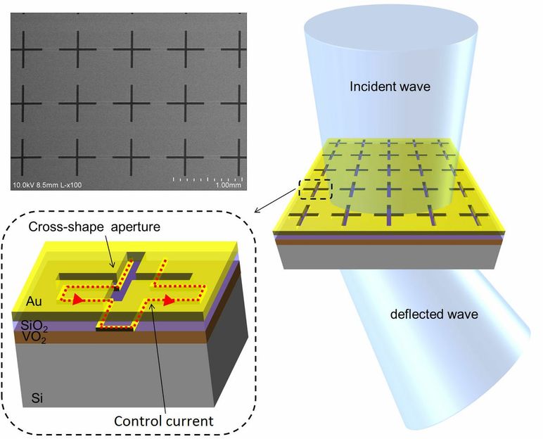
Figure showing how the metamaterial, with cross-chaped openings, can deflect a terahertz beam
UCLA
The material, specifically a metamaterial because it is has properties not found in nature, could be transformative for imaging, sensing and communication applications. It could be used for quality control in pharmaceutical production lines, scanning pills at high speeds to look for any defects; to spot cancerous tumors at early stages using tomography; or for forming adaptive high data-rate communication channels.
“Terahertz frequencies in particular offer some unique advantages, for example they can ‘see’ some details not otherwise ‘visible’ in other parts of the spectrum,” said Mona Jarrahi, an associate professor of electrical engineering at the UCLA Henry Samueli School of Engineering and Applied Science. “However their use is not widespread. Current systems require a mechanical scanning technique to steer or guide the focus area of the terahertz beam, much like a how an office copy machine uses a moving arm underneath the glass to capture an image.”
Despite extensive progress developing mechanical beam-steering techniques through miniaturization and the utilization of micro-electro mechanical systems, the potential use is still limited. Those tiny systems are complex with moving parts and for terahertz-based systems, they have not been practical. The team’s solution is simple.
“Our new metamaterial acts as a kind of moving lens that can focus on different areas of an object, but instead of being moved mechanically, its focus point is instead controlled electronically by changing an electric current that moves through it,” Jarrahi said. “The material itself never moves.”
The material is made up of metal-coated vanadium dioxide on silicon and is punctured with cross-shaped openings. It would be placed in front of the radiation beam used in an imaging or sensing application. Depending on the level of electric current, the material can deflect the beam’s focus point by as much as 44 degrees, both vertically and horizontally.
The new technology could lead to imaging, sensing and communication technologies in terahertz and far-infrared frequencies that are more reliable, compact, cost-effective and faster than the current state-of-the-art, the researchers said.
Original publication
Other news from the department science

Get the chemical industry in your inbox
By submitting this form you agree that LUMITOS AG will send you the newsletter(s) selected above by email. Your data will not be passed on to third parties. Your data will be stored and processed in accordance with our data protection regulations. LUMITOS may contact you by email for the purpose of advertising or market and opinion surveys. You can revoke your consent at any time without giving reasons to LUMITOS AG, Ernst-Augustin-Str. 2, 12489 Berlin, Germany or by e-mail at revoke@lumitos.com with effect for the future. In addition, each email contains a link to unsubscribe from the corresponding newsletter.
Most read news
More news from our other portals
Last viewed contents
Early Screening, Innovative Solutions to Underline Importance of ADME/Tox Technologies in Successful Drug Development - Considerable Time, Cost Savings to Accrue from Advanced ADME/Tox Technologies
Wacker Boosts Supply for Surface Coating Resins

Fueling the future - Scientists promote new method of algal hydrogen production

Ultraheavy precision polymers - Controlled photoenzymatic RAFT polymerization of nonconjugated polymers
New technique for detecting mold contamination in homes and other buildings
Gems_of_Sri_Lanka
Category:ADP_receptor_inhibitors

The dance of atoms
Clariant installs additional capacity at its emulsion plant in Argentina


