Obtaining of silicon nanowires becomes eco-friendly
Advertisement


Scientists from the Faculty of Physics, the Lomonosov Moscow State University have worked out a new and more eco-friendly method of silicon nanowires obtaining, which allows to replace hydrofluoric acid (HF) by ammonium fluoride (NH4F).
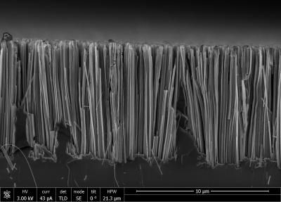
These silicon nanowires were obtained with the help of new eco-friendly method developed by Russian scientists. Toxic hydrofluoric acid is replaced by harmless ammonium fluoride.
Kirill Gonchar
Silicon nanowires are streamlined, almost parallel to each other nanostructures, looking like wires. Nanowires diameter varies from 50 to 200 nm, and the distance between structures - from 100 to 500 nm. Nanowires length, depending on etching time, could be from 100 nm and up to 10s of microns. Interest for silicon nanowires is caused by perspectives of their application in micro- and optoelectronics, photonics, PV, sensorics. They could be used even in biomedicine as silicon nanostructures are biodegradable materials, what means that they self-destruct in an organism after some period of time. Besides that, in limited concentrations nanostructures are not toxic for an organism. However, hydrofluoric acid (HF), used by conventional method in order to produce silicon nanowires, is extremely toxic.
Obtaining of silicon nanowires with the help of metal-assisted etching becomes possible due to chemical etching of a silicon wafer, where metal nanoparticles (for instance, silver nanoparticles) activate etching.
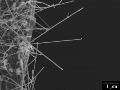
Kirill Gonchar, a Junior researcher in the Low Temperature Physics and Superconductivity Department, the Faculty of Physics, at the Lomonosov Moscow State University, describes the whole scheme of nanowires elaboration. He says: "We've used a two-step method of etching. At the first stage silver nanoparticles were deposited on the surface of a silicon wafer. But this deposition didn't produce a level layer but different island regions. At the second stage the silicon wafer was etched right in the places, covered with silver. Because of this, those silicone sheet places, which were uncovered with silver, turned into nanowires. Silver nanoparticles fell into the silicone sheet. And the more etching was lasting the longer nanowires were got at the output. At the end silver was removed with the help of nitric acid."
Researchers from the Lomonosov Moscow State University have replaced dangerous and toxic hydrofluoric acid by ammonium fluoride at all stages of chemical etching. Moreover, they have studied optical properties of silicon nanowires, produced with the help of this method, and compared them with nanowires, received on the basis of conventional method, rested on hydrofluoric acid usage.
Kirill Gonchar shares, how this idea to use ammonium fluoride in nanowires synthesis has emerged. He clarifies: "The idea of ammonium fluoride application wasn't new, it was borrowed from experiments of porous silicon obtaining, which took place 20 years ago. Ammonium fluoride was also used there instead of hydrofluoric acid. There were similar projects where nanowires were produced in ammonium fluoride, however, there was no replacement at all etching stages. We've studied optical properties of the nanowires we got and proved that they don't differ much from nanowires, obtained by conventional method."
Silicon nanowires, produced by metal-assisted etching, could be used for creation of new photonic devices and silicon based sensors. Kirill Gonchar clarifies, that nanowires are promising as sensory elements of optical sensors for different substances. This happens due to, first of all, increase of Raman effect signal intensity, which is a "finger print" of a substance. And, secondly, due to sensitivity to different gases presence, for instance, oxygen (the relevant patent has been already registered).
Moreover, structures, containing silicon nanowires, could be used in antireflection coating for solar cells. While ordinary silicon reflects in visible range about 30% of incident light, there could be obtained silicon nanowires which reflect 1-2%.


Other news from the department science


