Chemical etching method helps transistors stand tall
Smaller and faster has been the trend for electronic devices since the inception of the computer chip, but flat transistors have gotten about as small as physically possible. For researchers pushing for even faster speeds and higher performance, the only way to go is up.

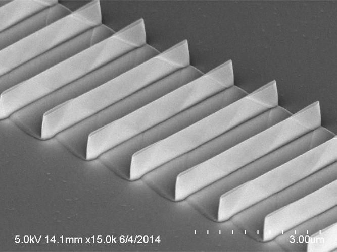
An array fin transistors made by the MacEtch method. The fins are tall and thin, with a higher aspect ratio and smoother sides than other methods can produce.
Yi Song, University of Illinois
University of Illinois researchers have developed a way to etch very tall, narrow finFETs, a type of transistor that forms a tall semiconductor "fin" for the current to travel over. The etching technique addresses many problems in trying to create 3-D devices, typically done now by stacking layers or carving out structures from a thicker semiconductor wafer.
"We are exploring the electronic device roadmap beyond silicon," said Xiuling Li, a U. of I. professor of electrical and computer engineering and the leader of the study. "With this technology, we are pushing the limit of the vertical space, so we can put more transistors on a chip and get faster speeds. We are making the structures very tall and smooth, with aspect ratios that are impossible for other existing methods to reach, and using a material with better performance than silicon."
Typically, finFETs are made by bombarding a semiconductor wafer with beams of high-energy ions. This technique has a number of challenges, Li said. For one, the sides of the fins are sloped instead of straight up and down, making them look more like tiny mountain ranges than fins. This shape means that only the tops of the fins can perform reliably. But an even bigger problem for high-performance applications is how the ion beam damages the surface of the semiconductor, which can lead to current leakage.
The Illinois technique, called metal-assisted chemical etching or MacEtch, is a liquid-based method, which is simpler and lower-cost than using ion beams, Li said. A metal template is applied to the surface, then a chemical bath etches away the areas around the template, leaving the sides of the fins vertical and smooth.
"We use a MacEtch technique that gives a much higher aspect ratio, and the sidewalls are nearly 90 degrees, so we can use the whole volume as the conducting channel," said graduate student Yi Song, the first author of the paper. "One very tall fin channel can achieve the same conduction as several short fin channels, so we save a lot of area by improving the aspect ratio."
The smoothness of the sides is important, since the semiconductor fins must be overlaid with insulators and metals that touch the tiny wires that interconnect the transistors on a chip. To have consistently high performance, the interface between the semiconductor and the insulator needs to be smooth and even, Song said.
Right now, the researchers use the compound semiconductor indium phosphide with gold as the metal template. However, they are working to develop a MacEtch method that does not use gold, which is incompatible with silicon.
"Compound semiconductors are the future beyond silicon, but silicon is still the industry standard. So it is important to make it compatible with silicon and existing manufacturing processes," Li said.
The researchers said the MacEtch technique could apply to many types of devices or applications that use 3-D semiconductor structures, such as computing memory, batteries, solar cells and LEDs.
Original publication
Other news from the department science

Get the chemical industry in your inbox
By submitting this form you agree that LUMITOS AG will send you the newsletter(s) selected above by email. Your data will not be passed on to third parties. Your data will be stored and processed in accordance with our data protection regulations. LUMITOS may contact you by email for the purpose of advertising or market and opinion surveys. You can revoke your consent at any time without giving reasons to LUMITOS AG, Ernst-Augustin-Str. 2, 12489 Berlin, Germany or by e-mail at revoke@lumitos.com with effect for the future. In addition, each email contains a link to unsubscribe from the corresponding newsletter.


