Quantum dot solids: This generation's silicon wafer?
Just as the single-crystal silicon wafer forever changed the nature of communication 60 years ago, a group of Cornell researchers is hoping its work with quantum dot solids - crystals made out of crystals - can help usher in a new era in electronics.
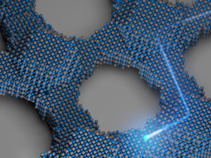
Connecting the dots: Playing 'LEGO' at the atomic scale to build atomically coherent quantum dot solids.
Kevin Whitham, Cornell University
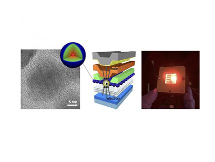
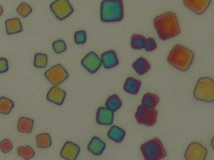
The team, led by Tobias Hanrath, associate professor in the Robert Frederick Smith School of Chemical and Biomolecular Engineering, and graduate student Kevin Whitham, has fashioned two-dimensional superstructures out of single-crystal building blocks. Through a pair of chemical processes, the lead-selenium nanocrystals are synthesized into larger crystals, then fused together to form atomically coherent square superlattices.
The difference between these and previous crystalline structures is the atomic coherence of each 5-nanometer crystal. They're not connected by a substance between each crystal - they're connected to each other. The electrical properties of these superstructures potentially are superior to existing semiconductor nanocrystals, with anticipated applications in energy absorption and light emission.
"As far as level of perfection, in terms of making the building blocks and connecting them into these superstructures, that is probably as far as you can push it," Hanrath said, referring to the atomic-scale precision of the process.
This latest work has grown out of previous published research by the Hanrath group, that reported a new approach to connecting quantum dots through controlled displacement of a connector molecule, called a ligand. That paper referred to "connecting the dots" - i.e. electronically coupling each quantum dot - as being one of the most persistent hurdles to be overcome.
That barrier seems to have been cleared with this new research. The strong coupling of the nanocrystals leads to formation of energy bands that can be manipulated based on the crystals' makeup, and could be the first step toward discovering and developing other artificial materials with controllable electronic structure.
Still, Whitham said, more work must be done to bring the group's work from the lab to society. The structure of the Hanrath group's superlattice, while superior to ligand-connected nanocrystal solids, still has multiple sources of disorder due to the fact that all nanocrystals are not identical. This creates defects, which limit electron wave function.
"I see this paper as sort of a challenge for other researchers to take this to another level," Whitham said. "This is as far as we know how to push it now, but if someone were to come up with some technology, some chemistry, to provide another leap forward, this is sort of challenging other people to say, 'How can we do this better?'"
Hanrath said the discovery can be viewed in one of two ways, depending on whether you see the glass as half empty or half full.
"It's the equivalent of saying, 'Now we've made a really large single-crystal wafer of silicon, and you can do good things with it,'" he said, referencing the game-changing communications discovery of the 1950s. "That's the good part, but the potentially bad part of it is, we now have a better understanding that if you wanted to improve on our results, those challenges are going to be really, really difficult."
Original publication
Other news from the department science
Get the chemical industry in your inbox
By submitting this form you agree that LUMITOS AG will send you the newsletter(s) selected above by email. Your data will not be passed on to third parties. Your data will be stored and processed in accordance with our data protection regulations. LUMITOS may contact you by email for the purpose of advertising or market and opinion surveys. You can revoke your consent at any time without giving reasons to LUMITOS AG, Ernst-Augustin-Str. 2, 12489 Berlin, Germany or by e-mail at revoke@lumitos.com with effect for the future. In addition, each email contains a link to unsubscribe from the corresponding newsletter.
