Designer crystals for next-gen electronics
Liquid is often seen as the kryptonite of electronics, known for damaging and corroding components. That's why a new process that uses vapour- rather than liquid - to grow designer Crystals could lead to a new breed of faster, more powerful electronic devices. The method, invented by an international team of scientists from the University of Leuven in Belgium, the National University of Singapore and CSIRO has been published.
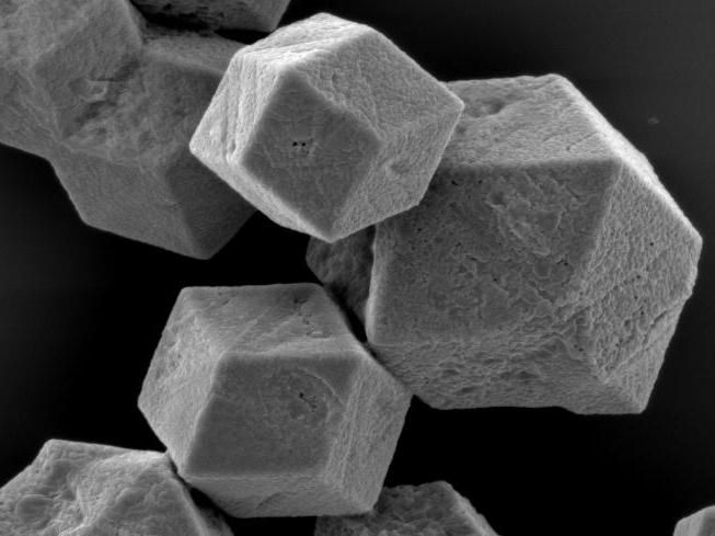
This is a close up of the metal organic framework crystals.
CSIRO
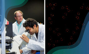
For the first time, the researchers have shown how the designer crystals known as 'metal organic frameworks' or MOFs, can be grown using a vapour method that is similar to steam hovering over a pot of hot water. The crystals are the world's most porous materials, and if applied to microelectronic devices, could significantly boost their processing power. However according to CSIRO researcher Mark Styles (right), up until now these crystals could only be grown and applied using a liquid solvent, making them unsuitable for electronics applications.
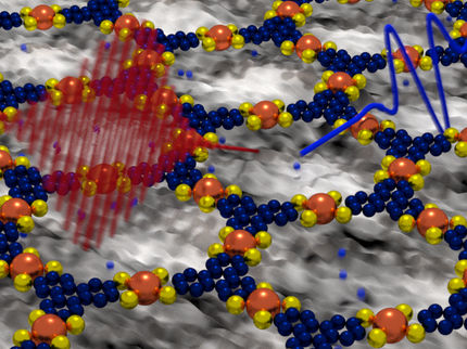
"Just like your smart phone doesn't like being dropped in water, electronic devices don't like the liquid solvent that's used to grow MOF crystals," Dr Styles said. "It can corrode and damage the delicate circuitry. Our new vapour method for growing and applying MOF crystals overcomes this barrier and has the potential to disrupt the microelectronics industry. On the atomic scale, MOF crystals look like bird cages that can be tailor-made to be different shapes and sizes. They have an extremely large surface area, meaning they can be up to 80 per cent empty inside. The net result is a structure where almost every atom is exposed to empty space: one gram of MOF crystals has a surface area of over 5000 square metres - that's the size of a football field. Crucially, we can use this vast space to trap other molecules, which can change the properties of a material. In the case of electronics, this means we can fit a lot more transistors on a microchip, making it faster and far more powerful."
The international team, which was led by Ivo Stassen and Professor Rob Ameloot from the University of Leuven in Belgium, drew on specialist X-ray analysis techniques from CSIRO and the Australian Synchrotron to understand how the vapour process works, and how it can be used to grow the MOF crystals.
According to Dr Styles, the applications for MOFs can only be limited by your imagination.
"Another potential use for this technology would be in portable chemical sensing devices that could be used in hazardous environments such as chemical processing plants and underground mines," he said.
Original publication
Original publication
Ivo Stassen, Mark Styles, Gianluca Grenci, Hans Van Gorp, Willem Vanderlinden, Steven De Feyter, Paolo Falcaro, Dirk De Vos, Philippe Vereecken & Rob Ameloot; "Chemical vapour deposition of zeolitic imidazolate framework thin films"; Nature Materials; 2015
Organizations
Other news from the department science

Get the chemical industry in your inbox
By submitting this form you agree that LUMITOS AG will send you the newsletter(s) selected above by email. Your data will not be passed on to third parties. Your data will be stored and processed in accordance with our data protection regulations. LUMITOS may contact you by email for the purpose of advertising or market and opinion surveys. You can revoke your consent at any time without giving reasons to LUMITOS AG, Ernst-Augustin-Str. 2, 12489 Berlin, Germany or by e-mail at revoke@lumitos.com with effect for the future. In addition, each email contains a link to unsubscribe from the corresponding newsletter.
