A new slant on semiconductor characterization
Advertisement


From laptops and televisions to smartphones and tablets, semiconductors have made advanced electronics possible. These types of devices are so pervasive, in fact, that Northwestern Engineering's Matthew Grayson says we are living in the "Semiconductor Age."
"You have all these great applications like computer chips, lasers, and camera imagers," said Grayson, associate professor of electrical engineering and computer science in Northwestern's McCormick School of Engineering. "There are so many applications for semiconductor materials, so it's important that we can characterize these materials carefully and accurately. Non-uniform semiconductors lead to computer chips that fail, lasers that burn out, and imagers with dark spots."
Grayson's research team has created a new mathematical method that has made semiconductor characterization more efficient, more precise, and simpler. By flipping the magnetic field and repeating one measurement, the method can quantify whether or not electrical conductivity is uniform across the entire material - a quality required for high-performance semiconductors.
"Up until now, everyone would take separate pieces of the material, measure each piece, and compare differences to quantify non-uniformity," Grayson said. "That means you need more time to make several different measurements and extra material dedicated for diagnostics. We have figured out how to measure a single piece of material in a magnetic field while flipping the polarity to deduce the average variation in the density of electrons across the sample."
Remarkably, the contacts at the edge of the sample reveal information about the variations happening throughout the body of the sample.
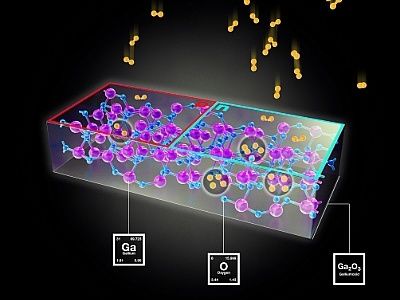
One reason semiconductors have so many applications is because researchers and manufacturers can control their properties. By adding impurities to the material, researchers can modulate the semiconductor's electrical properties. The trick is making sure that the material is uniformly modulated so that every part of the material performs equally well. Grayson's technique allows researchers and manufacturers to directly quantify such non-uniformities.
"When people see non-uniform behavior, sometimes they just throw out the material to find a better piece," Grayson said. "With our information, you can find a piece of the material that's more uniform and can still be used. Or you can use the information to figure out how to balance out the next sample."
Grayson's method can be applied to samples as large as a 12-inch wafer or as small as an exfoliated 10-micron flake, allowing researchers to profile the subtleties in a wide range of semiconductor samples. The method is especially useful for 2-D materials, such as graphene, which are too small for researchers to make several measurements across the surface.
Grayson has filed a patent on the method, and he hopes the new technique will find use in academic laboratories and industry.
"There are companies that mass produce semiconductors and need to know if the material is uniform before they start making individual computer chips," Grayson said. "Our method will give them better feedback during sample preparation. We believe this is a fundamental breakthrough with broad impact."
Original publication


Other news from the department science


