Scientists demonstrate how to improve ultrathin CIGSe solar cells by nanoparticles
CIGSe solar cells are made of a thin chalcopyrite layer consisting of copper, indium, gallium and selenium and can reach high efficiencies. Since Indium is becoming scarce and expensive, it is interesting to reduce the active CIGSe layer, which however decreases the efficiency quite strongly. Now, scientists at Helmholtz-Zentrum Berlin have produced high quality ultrathin CIGSe layers and increased their efficiency by an array of tiny nanoparticles between the back contact and the active layer.
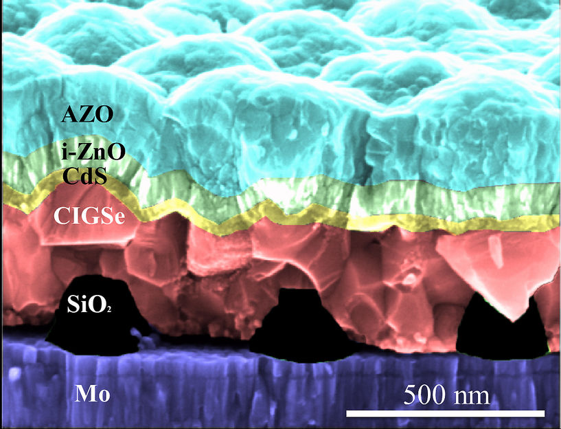
The SiO2 nanoparticles (black) have been imprinted directly on the Molybdenum substrate (purple) which corresponds to the back contact of the solar cell. On top of this structured substrate the ultrathin CIGSe layer (red) was grown at HZB, and subsequently all the other layers and contacts needed for the solar cell. Since all layers are extremely thin, even the top layer is showing deformations according to the pattern of the nanoparticles.
G.Yin/HZB
Nanoparticles with sizes the order of a wavelength interact with light in specific ways. A young investigator group at Helmholtz-Zentrum Berlin, led by Professor Martina Schmid, is inquiring how to use arrangements of such nanoparticles to improve solar cells and other opto-electronic devices. Now the scientists report in the Journal of the American Chemical Society ACS Nano a considerable success with ultrathin CIGSe solar cells.
Problems add up below 1 micrometer
CIGSe solar cells have proven high efficiencies and are established thin film devices with active layers of a few micrometers thickness. But since Indium is a rare element, the active layer should be as thin as possible. This reduces the efficiency, since less light is absorbed. And if the active layer is thinner than one micrometer, an additional problem arises: more and more charge carriers meet and recombine at the back contact, getting “lost”.
Ultrathin CIGSe cell with efficiencies of 11.1%
“It took me more than one year to be able to produce ultrathin layers of only 0.46 micrometer or 460 nanometers which still reach reasonable efficiencies up to 11.1 %,” Guanchao Yin says about his PhD project. He then started to enquire how to implement nanoparticles between different layers of the solar cell. His supervisor Martina Schmid discussed this with Prof. Albert Polman, one of the pioneers in the field of nanophotonics, at the Center for Nanooptics, Amsterdam, with whom she was in contact for a while already. They proposed to produce arrays of dielectric nanoparticles by nanoimprinting technologies.
No big effect by nanoparticles on top
In a first step, the colleagues in Amsterdam implemented a pattern of dielectric TiO2-nanoparticles on top of Yin’s ultrathin solar cells; the idea was that they would act as light traps and increase absorption in the CIGSe layer. But this did not increase the efficiency as much as proved in Si-based solar cells. Yin then continued testing and ultimately found out what worked best: a nanoparticle array not on top but at the back contact of the cell!
Nanoparticles at the back contact: effiency increases to 12.3%
The colleagues from Amsterdam produced an array of SiO2 nanoparticles, directly on the Molybdenum substrate which corresponds to the back contact of the solar cell. On top of this structured substrate the ultrathin CIGSe layer was grown by Yin, and subsequently all the other layers and contacts needed for the solar cell. With this configuration, the efficiency increased from 11.1 % to 12.3 %, and the short circuit current density of the ultrathin CIGSe cells increased by more than 2 mA/cm2. With additional anti-reflective nanoparticles at the front efficiencies raised even to 13.1%.
Light trapping and prevention of charge carrier loss
“This leads to efficient light trapping and does not deteriorate the cell,” Yin explains. Further studies indicate that the nanoarray of dielectric SiO2 nanoparticles at the back side could also increase efficiency by reducing chances for charge carrier recombination. “This work is just a start, we have now new ideas for further designs to enhance absorption and reduce recombination, thus increasing efficiencies by making use of optical and electrical benefits of the nanoparticles,” Martina Schmid says.
Original publication
Other news from the department science
These products might interest you
NANOPHOX CS by Sympatec
Particle size analysis in the nano range: Analyzing high concentrations with ease
Reliable results without time-consuming sample preparation

Eclipse by Wyatt Technology
FFF-MALS system for separation and characterization of macromolecules and nanoparticles
The latest and most innovative FFF system designed for highest usability, robustness and data quality

DynaPro Plate Reader III by Wyatt Technology
Screening of biopharmaceuticals and proteins with high-throughput dynamic light scattering (DLS)
Efficiently characterize your sample quality and stability from lead discovery to quality control

Get the chemical industry in your inbox
By submitting this form you agree that LUMITOS AG will send you the newsletter(s) selected above by email. Your data will not be passed on to third parties. Your data will be stored and processed in accordance with our data protection regulations. LUMITOS may contact you by email for the purpose of advertising or market and opinion surveys. You can revoke your consent at any time without giving reasons to LUMITOS AG, Ernst-Augustin-Str. 2, 12489 Berlin, Germany or by e-mail at revoke@lumitos.com with effect for the future. In addition, each email contains a link to unsubscribe from the corresponding newsletter.
