Nanoscale photodetector shows promise to improve the capacity of photonic circuits
Advertisement
photonic circuits, which use light to transmit signals, are markedly faster than electronic circuits. Unfortunately, they're also bigger. It's difficult to localize visible light below its diffraction limit, about 200-300 nanometers, and as components in electronic semiconductors have shrunk to the nanometer scale, the photonic circuit size limitation has given electronic circuits a significant advantage, despite the speed discrepancy.

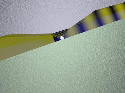
This image shows light traveling along a silver nanowire as plasmons and re-emitted via molybdenum disulfide.
M. Osadciw, University of Rochester, New York
Now researchers at the University of Rochester have demonstrated a key achievement in shrinking photonic devices below the diffraction limit - a necessary step on the road to making photonic circuits competitive with today's technology. The scientists developed a nanoscale photodetector that uses the common material molybdenum disulfide to detect optical plasmons - travelling oscillations of electrons below the diffraction limit - and successfully demonstrated that light can drive a current using a silver nanowire.
"Our devices are a step towards miniaturization below the diffraction limit," said Kenneth Goodfellow, a graduate student in the laboratory of the Quantum Optoelectronics and Optical Metrology Group, The Institute of Optics, University of Rochester, New York. "It is a step towards using light to drive, or, at least complement electronic circuitry for faster information transfer."
The device expands on previous work demonstrating that light could be transmitted along a silver nanowire as a plasmon and re-emitted at the other end, which was covered with atomically-thin flakes of molybdenum disulfide (MoS2). When re-emitted, the light corresponded to the band gap of MoS2, rather than solely to the laser's wavelength, demonstrating that the plasmons effectively nudged the electrons in MoS2into a different energy state.
"The natural next idea would be to see if this type of device would be able to be used as a photodetector," Goodfellow said.
To do this, the group transferred a silver nanowire coated at one end with MoS2 onto a silicon substrate and deposited metal contacts onto that same end with electron beam lithography. They then connected the device to equipment to control its bias, or fixed, voltage and to measure the current running through it.
When the uncovered end of the wire was exposed to a laser, the energy was converted into plasmons, a form of electromagnetic wave that travels through oscillations in electron density. This energy electronically excited an electron once it reached the molybdenum disulfide-covered end, effectively generating a current.
By scanning the wire bit-by-bit with a laser -- a process known as raster scanning -- the researchers were able to measure current at each point along the wire, finding that it was sensitive to the polarization of the incoming light and was at its strongest when the light was polarized parallel to the wire. They also found that the device was sensitive to the laser's excitation wavelength, and performance was limited at shorter wavelengths due to ineffective plasmon propagation and at longer wavelengths due to the band gap of molybdenum disulfide.
"Full photonic circuits are some time in the future, but this work helps to feed the current effort," Goodfellow said.


