How specific atoms move in dielectric materials
Researchers from North Carolina State University, the National Institute of Standards and Technology (NIST), and UNSW Australia have measured the behavior of specific atoms in dielectric materials when exposed to an electric field. The work advances our understanding of dielectric materials, which are used in a wide variety of applications - from handheld electronics to defibrillators.

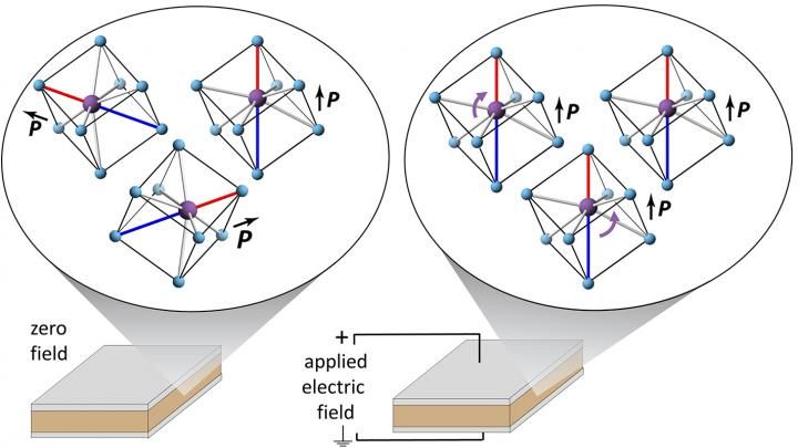
Researchers have measured how the atoms within electrically insulating solids reorient due to an applied electric field. Shown here for Na1/2Bi1/2TiO3, bismuth ions (purple) align along the electric field direction relative to their surrounding titanium ions (blue). Oxygen ions not shown.
Tedi-Marie Usher
"Dielectric materials are insulators that can store and manage electric charge. But we hadn't yet directly measured how atoms move in dielectric materials in order to store that charge," says Tedi-Marie Usher, a Ph.D. candidate in materials science and engineering at NC State and lead author of a paper on the work.
To get to the bottom of this problem, the researchers applied voltage to a dielectric material, creating an electric field. They simultaneously bombarded the material with X-rays from a synchrotron at Argonne National Laboratory's Advanced Photon Source. When the X-rays hit the material, they scatter into a pattern of bright rings. Typically, to figure out the arrangement of atoms in a material, the positions and intensities of these bright rings are analyzed.
However, by applying new mathematical techniques that are more sensitive to the weak (dim) scattered X-rays, the researchers could determine changes in the placement of specific atoms within the crystalline structure of the material. In other words, the researchers could "see" how the atoms moved relative to each other in response to the electric field.
"A good analogy would be that analyzing the bright rings is like examining a skyscraper from far away and determining that each office is 500 square feet. However, by also analyzing the weak X-rays scattered from the sample, we can determine that some offices are 400 square feet and others are 600 square feet, and some have the desk on the east side, and others have the desk on the north side," says Usher. This is an uncommon approach, because experimenters typically only evaluate the bright rings.
"What's really new here is that this technique is much more sensitive to the behavior of select atoms relative to their neighboring atoms, rather than looking at an average of all the atoms in a sample," says Jacob Jones, a professor of materials science and engineering at NC State and corresponding author of the paper.
The work uses a technique called a pair distribution function, which allows researchers to extract information about how atoms are arranged at extremely small length-scales based on the weak intensity X-rays diffracted from a sample. The researchers evaluated three different dielectric materials for this study.
"One of the interesting findings here is that each of the three dielectric materials we tested exhibited very different behaviors at the atomic level - there was no single atomic behavior that accounted for dielectric properties across the materials," Jones says.
For example, the researchers tested a material called sodium bismuth titanate - a non-toxic material that is thought to be promising for use in dielectric devices. In the absence of an electric field, researchers knew that the bismuth ions are off-center relative to neighboring atoms. But different bismuth ions would be off-center in different directions. However, when an electric field is applied, virtually all of the bismuth ions shifted so they were off-center in the same direction as the electric field.
"Neither of the other dielectric materials exhibited similar behavior," Usher says. "One of our questions for future work is whether the bismuth behavior we saw in sodium bismuth titanate is consistent across bismuth-based dielectrics."
"We also want to know how dielectric materials and other complex materials, such as high-entropy alloys, behave at the atomic scale when under mechanical stress," Jones says.
Original publication
Other news from the department science

Get the chemical industry in your inbox
By submitting this form you agree that LUMITOS AG will send you the newsletter(s) selected above by email. Your data will not be passed on to third parties. Your data will be stored and processed in accordance with our data protection regulations. LUMITOS may contact you by email for the purpose of advertising or market and opinion surveys. You can revoke your consent at any time without giving reasons to LUMITOS AG, Ernst-Augustin-Str. 2, 12489 Berlin, Germany or by e-mail at revoke@lumitos.com with effect for the future. In addition, each email contains a link to unsubscribe from the corresponding newsletter.
Most read news
More news from our other portals
Last viewed contents
Kemira strengthens its growing water and environment business by acquiring Galvatek

Reusable carbon nanotubes could be the water filter of the future
Merger of Nihon Green & Garden with Hodogaya Agros
Agilent Technologies extends boundaries of environmental metals analysis
Evonik increases prices for DEGALAN® in NAFTA
WeylChem to Produce Grignard Reagents On An Industrial Scale - Custom Chemical Manufacturing Company Diversifies To Include Functional Products
MorphoSys Co-Founder And Member Of The Board Receives Award For Outstanding Scientific Achievements


