Researchers Develop Ultrahigh-Resolution 3D Microscopy Technique for Electric Fields
Down to the Quantum Dot
Using a single molecule as a sensor, scientists in Jülich have successfully imaged electric potential fields with unrivalled precision. The ultrahigh-resolution images provide information on the distribution of charges in the electron shells of single molecules and even atoms. The 3D technique is also contact-free. The first results achieved using "scanning quantum dot microscopy" have been published in the current issue of Physical Review Letters. The related publication was chosen as the Editor's suggestion and selected as a Viewpoint in the science portal Physics. The technique is relevant for diverse scientific fields including investigations into biomolecules and semiconductor materials.

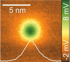
A single silver atom on a silver substrate (Ag(111)) under the scanning quantum dot microscope.
Forschungszentrum Jülich

Left: The scanning quantum dot micrograph of a PTCDA molecule reveals the negative partial charges at the ends of the molecule as well as the positive partial charges in the centre. Centre: Simulated electric potential above a PTCDA molecule with molecular structure Right: Schematic of charge distribution in the PTCDA molecule.
Forschungszentrum Jülich

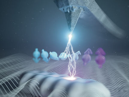
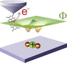
Illustration of the measuring principle: depending on the local electric potential field of a nanostructure on the surface of a sample, a single electron jumps from the tip of the microscope to the sensor molecule or back.
Forschungszentrum Jülich

"Our method is the first to image electric fields near the surface of a sample quantitatively with atomic precision on the sub-nanometre scale," says Dr. Ruslan Temirov from Forschungszentrum Jülich. Such electric fields surround all nanostructures like an aura. Their properties provide information, for instance, on the distribution of charges in atoms or molecules.
For their measurements, the Jülich researchers used an atomic force microscope. This functions a bit like a record player: a tip moves across the sample and pieces together a complete image of the surface. To image electric fields up until now, scientists have used the entire front part of the scanning tip as a Kelvin probe. But the large size difference between the tip and the sample causes resolution difficulties – if we were to imagine that a single atom was the same size as a head of a pin, then the tip of the microscope would be as large as the Empire State Building.
Single molecule as a sensor
In order to improve resolution and sensitivity, the scientists in Jülich attached a single molecule as a quantum dot to the tip of the microscope. Quantum dots are tiny structures, measuring no more than a few nanometres across, which due to quantum confinement can only assume certain, discrete states comparable to the energy level of a single atom.
The molecule at the tip of the microscope functions like a beam balance, which tilts to one side or the other. A shift in one direction or the other corresponds to the presence or absence of an additional electron, which either jumps from the tip to the molecule or does not. The "molecular" balance does not compare weights but rather two electric fields that act on the mobile electron of the molecular sensor: the first is the field of a nanostructure being measured, and the second is a field surrounding the tip of the microscope, which carries a voltage.
"The voltage at the tip is varied until equilibrium is achieved. If we know what voltage has been applied, we can determine the field of the sample at the position of the molecule," explains Dr. Christian Wagner, a member of Temirov’s Young Investigators group at Jülich’s Peter Grünberg Institute (PGI-3). "Because the whole molecular balance is so small, comprising only 38 atoms, we can create a very sharp image of the electric field of the sample. It’s a bit like a camera with very small pixels."
Universally applicable
A patent is pending for the method, which is particularly suitable for measuring rough surfaces, for example those of semiconductor structures for electronic devices or folded biomolecules. "In contrast to many other forms of scanning probe microscopy, scanning quantum dot microscopy can even work at a distance of several nanometres. In the nanoworld, this is quite a considerable distance," says Christian Wagner. Until now, the technique developed in Jülich has only been applied in high vacuum and at low temperatures: essential prerequisites to carefully attach the single molecule to the tip of the microscope.
"In principle, variations that would work at room temperature are conceivable," believes the physicist. Other forms of quantum dots could be used as a sensor in place of the molecule, such as those that can be realized with semiconductor materials: one example would be quantum dots made of nanocrystals like those already being used in fundamental research.
