Two-dimensional semiconductor comes clean
In 2013 James Hone, Wang Fong-Jen Professor of Mechanical Engineering at Columbia Engineering, and colleagues at Columbia demonstrated that they could dramatically improve the performance of graphene - highly conducting two-dimensional (2D) carbon - by encapsulating it in boron nitride (BN), an insulating material with a similar layered structure. In work published on Nature Nanotechnology's website, researchers at Columbia Engineering, Harvard, Cornell, University of Minnesota, Yonsei University in Korea, Danish Technical University, and the Japanese National Institute of Materials Science have shown that the performance of another 2D material - molybdenum disulfide (MoS2) - can be similarly improved by BN-encapsulation.
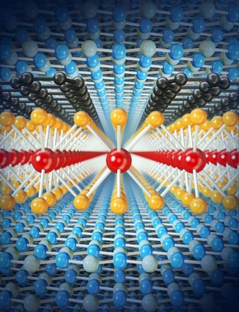
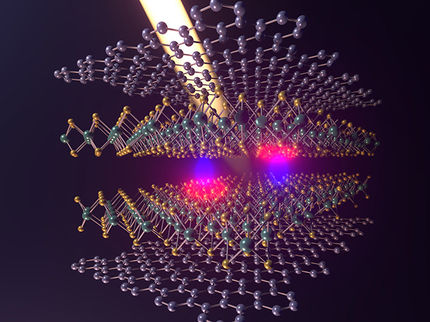
This is a schematic cross-section view of atomic layer of molybdenum disulfide contacted by graphene, and encapsulated between layers of insulating hexagonal boron nitride.
Gwan-Hyoung Lee/Columbia Engineering
"These findings provide a demonstration of how to study all 2D materials," says Hone, leader of this new study and director of Columbia's NSF-funded Materials Research Science and Engineering Center. "Our combination of BN and graphene electrodes is like a 'socket' into which we can place many other materials and study them in an extremely clean environment to understand their true properties and potential. This holds great promise for a broad range of applications including high-performance electronics, detection and emission of light, and chemical/bio-sensing."
Two-dimensional (2D) materials created by "peeling'" atomically thin layers from bulk crystals are extremely stretchable, optically transparent, and can be combined with each other and with conventional electronics in entirely new ways. But these materials--in which all atoms are at the surface--are by their nature extremely sensitive to their environment, and their performance often falls far short of theoretical limits due to contamination and trapped charges in surrounding insulating layers. The BN-encapsulated graphene that Hone's group produced last year has 50× improved electronic mobility--an important measure of electronic performance--and lower disorder that enables the study of rich new phenomena at low temperature and high magnetic fields.
"We wanted to see what we could do with MoS2--it's the best-studied 2D semiconductor, and, unlike graphene, it can form a transistor that can be switched fully 'off', a property crucial for digital circuits," notes Gwan-Hyoung Lee, co-lead author on the paper and assistant professor of materials science at Yonsei. In the past, MoS2 devices made on common insulating substrates such as silicon dioxide have shown mobility that falls below theoretical predictions, varies from sample to sample, and remains low upon cooling to low temperatures, all indications of a disordered material. Researchers have not known whether the disorder was due to the substrate, as in the case of graphene, or due to imperfections in the material itself.
In the new work, Hone's team created heterostructures, or layered stacks, of MoS2 encapsulated in BN, with small flakes of graphene overlapping the edge of the MoS2 to act as electrical contacts. They found that the room-temperature mobility was improved by a factor of about 2, approaching the intrinsic limit. Upon cooling to low temperature, the mobility increased dramatically, reaching values 5-50× that those measured previously (depending on the number of atomic layers). As a further sign of low disorder, these high-mobility samples also showed strong oscillations in resistance with magnetic field, which had not been previously seen in any 2D semiconductor.
"This new device structure enables us to study quantum transport behavior in this material at low temperature for the first time," added Columbia Engineering PhD student Xu Cui, the first author of the paper.
By analyzing the low-temperature resistance and quantum oscillations, the team was able to conclude that the main source of disorder remains contamination at the interfaces, indicating that further improvements are possible.
"This work motivates us to further improve our device assembly techniques, since we have not yet reached the intrinsic limit for this material," Hone says. "With further progress, we hope to establish 2D semiconductors as a new family of electronic materials that rival the performance of conventional semiconductor heterostructures--but are created using scotch tape on a lab-bench instead of expensive high-vacuum systems."
Organizations
Other news from the department science

Get the chemical industry in your inbox
By submitting this form you agree that LUMITOS AG will send you the newsletter(s) selected above by email. Your data will not be passed on to third parties. Your data will be stored and processed in accordance with our data protection regulations. LUMITOS may contact you by email for the purpose of advertising or market and opinion surveys. You can revoke your consent at any time without giving reasons to LUMITOS AG, Ernst-Augustin-Str. 2, 12489 Berlin, Germany or by e-mail at revoke@lumitos.com with effect for the future. In addition, each email contains a link to unsubscribe from the corresponding newsletter.
Most read news
More news from our other portals
Last viewed contents
Molecular switch for cheaper biofuel
Triboelectric nanogenerators boost mass spectrometry performance

