Defects are perfect in laser-induced graphene
Rice University lab discovers simple way to make material for energy storage, electronics
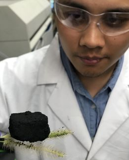
Researchers at Rice University have created flexible, patterned sheets of multilayer graphene from a cheap polymer by burning it with a computer-controlled laser. The process works in air at room temperature and eliminates the need for hot furnaces and controlled environments, and it makes graphene that may be suitable for electronics or energy storage.
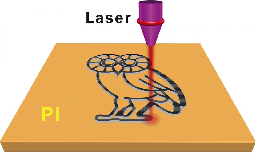
A Rice University lab is using a laser to write graphene microsupercapacitors in a common polymer material. The laser removes nearly everything but carbon from a 20-micron layer, leaving behind porous graphene foam that may be suitable for electronics or energy storage.
Tour Group/Rice University
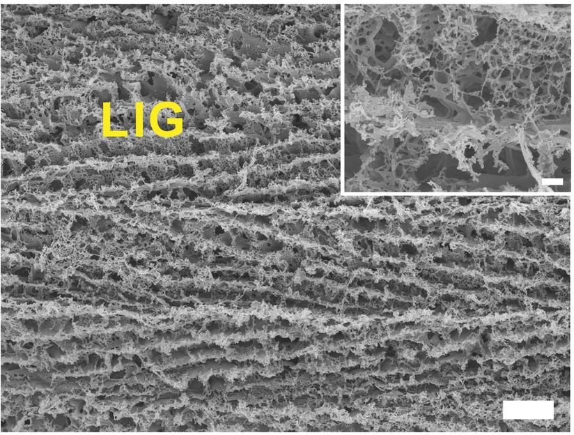
A scanning electron microscope shows a close-up of laser-induced graphene foam produced by researchers at Rice University. The scale bar for the main image is 10 microns; the bar for the inset is 1 micron.
Tour Group/Rice University

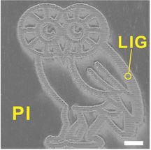
This finely detailed Rice Owl was produced by burning a graphene foam pattern into a flexible polyimide sheet with a laser. The multilayered graphene that results from the process may be suitable for energy storage or electronics. The scale bar is 1 millimeter.
Tour Group/Rice University
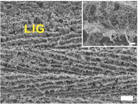
Under a microscope, what the researchers call laser-induced graphene (LIG) doesn't look like a perfect chicken wire-like grid of atoms. Instead, it's a jumble of interconnected graphene flakes with five-, six- and seven-atom rings. The paired five- and seven-atom rings are considered defects - but in this case, they're not. They're features.
The material can be made in detailed patterns. For show-and-tell, the Rice team patterned millimeter-sized LIG Owls (the school's mascot), and for practical testing they fabricated microscale supercapacitors with LIG electrodes in one-step scribing. The labs of Rice chemist James Tour and theoretical physicist Boris Yakobson published their research in Nature Communications.
The one-step process is scalable, said Tour, who suggested it could allow for rapid roll-to-roll manufacture of nanoscale electronics.
"This will be good for items people can relate to: clothing and wearable electronics like smartwatches that configure to your smartphone," he said.
This top-down approach to making graphene is quite different from previous works by Tour's lab, which pioneered the small-scale manufacture of the atom-thick material from common carbon sources, even Girl Scout cookies, and learned to split multiwalled nanotubes into useful graphene nanoribbons.
But as in the previous work, the base material for LIG is inexpensive. "You buy polyimide flexible plastic sheets in huge rolls, called Kapton, and the process is done entirely in air with a rapid writing process. That sets it up for a very scalable, industrial process," Tour said.
The product is not a two-dimensional slice of graphene but a porous foam of interconnected flakes about 20 microns thick. The laser doesn't cut all the way through, so the foam remains attached to a manageable, insulating, flexible plastic base.
The process only works with a particular polymer. The researchers led by Jian Lin, a former postdoctoral research in the Tour Group and now an assistant professor at the University of Missouri, tried 15 different polymers and found only two could be converted to LIG. Of those, polyimide was clearly the best.
Tour said the resulting graphene isn't as conductive as copper, but it doesn't need to be. "It's conductive enough for many applications," he said.
He said LIG can easily be turned into a supercapacitor, which combines the fast-charging, power-storing capacity of a capacitor with the higher energy-delivering capability, though not yet as high as in a battery. The defects could be the key, Tour said.
"A normal sheet of graphene is full of six-member rings," he said. "Once in a while you see a meandering line of 5-7s, but this new material is filled with 5-7s. It's a very unusual structure, and these are the domains that trap electrons. Had it just been normal (highly conductive) graphene, it couldn't store a charge."
Calculations by Yakobson's group showed that these balancing five-and-seven formations make the material more metallic and enhance its ability to store charges.
"Theoretical methods and density functional computations allowed us to look inside the electronic energy states' organization," Yakobson said. "What we discovered is that the very low density of available states -- which is crucial for the layer capacitance -- increases dramatically, due to various topological defects, mainly pentagonal and heptagonal rings.
"The fact that highly defective graphene performs so well is a freebie, a gift from nature," he said.
