Slow-motion movies of tiny nanostructures
Researchers developed a novel microscope
Advertisement
Physicists from the University of Regensburg have developed a novel microscope that allows them to record slow-motion movies of tiny nanostructures with groundbreaking time resolution – faster even than a single oscillation cycle of light. With their new microscope they have directly imaged the super-fast motion of electrons, which has now been published in “Nature Photonics”.
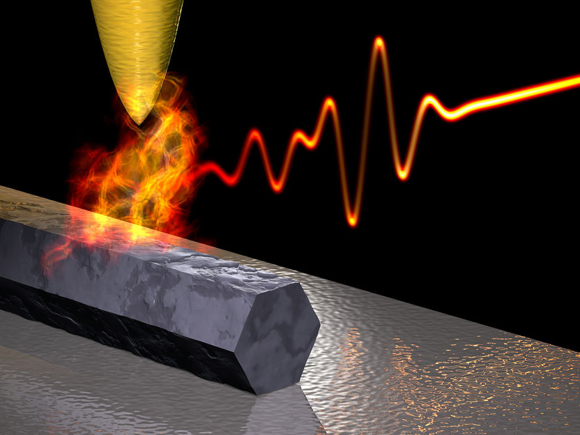
Schematic representation of the new microscope imaging super-fast motions of electrons.
Max Eisele
Modern nanotechnology does what nature has always been able to do: Systematic structuring on the nanometer length scale – the billionth part of a meter – to create artificial materials with novel properties. Important examples are semiconductor building blocks for high-speed electronics. To understand the behavior of these structures and to make them even faster, smaller, and more efficient, scientists would like to trace directly how electrons move on length scales of only a few atoms. These processes often occur extremely quickly, which has spurred a drive to develop a microscope that combines excellent spatial resolution with the highest possible temporal resolution. Max Eisele, Tyler Cocker et collegues at the Institute for Experimental and Applied Physics at the University of Regensburg have now developed a microscope that fulfills such requirements.
The physicists achieve excellent spatial resolution by focusing light onto a tiny metal tip. The tip collects and confines the light to a volume only 10 nanometers wide in all three spatial dimensions – a volume that is a billion times smaller than in conventional optical microscopy. The tip is then raster scanned over a sample surface and the incident light that is scattered depends upon the local properties of the sample directly below the tip. The group illuminates the tip with infrared flashes of light only a few femtoseconds in duration. A femtosecond is the unbelievably short temporal duration of a billionth part of a millionth of a second. To detect the scattered light with the highest possible temporal resolution the physicists use incredibly fast sensors that can even observe the oscillations of infrared light.
Like in slow-motion movies, these light flashes allow the researchers to take snapshots of super-fast electronic nano-motion. In a spectacular demonstration experiment the scientists were able to record a 3D movie of electrons moving at the surface of a semiconductor nanowire, which was only accessible in an indirect way up until now.
Such nanostructures, which have been fabricated at the CNR - Istituto Nanoscienze in Pisa, are of great interest for future high-speed electronics. Besides answering technological questions in electronics and photovoltaics, the microscope will also be valuable for a wide range of interdisciplinary applications, which range from providing novel physical insights into exotic materials to understanding biological processes on the molecular scale.


