Using strain to tune a new quantum material
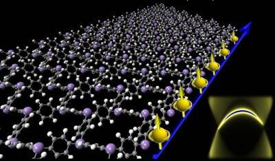
Research into a recently discovered class of materials shows they have the necessary characteristics to develop ultra-energy efficient electronics. Topological insulators (TI) are three-dimensional materials that conduct electricity on their surfaces, while the interior insulates.

University of Wisconsin - Milwaukee
Their surfaces are particularly unique because the motion of the electrons is "protected" by symmetry, meaning electrons will keep moving without scattering even when they encounter defects and contamination.
In fact, electrons on the surface of TIs move so robustly scientists are trying to determine the best way to control or "tune" them in order to use them in next-generation electronics. Until now the only way to change the electronic state was to apply a magnetic or an electric field.
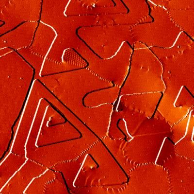
But research led by physicists at the University of Wisconsin-Milwaukee (UWM) has revealed a new method. The team proved that surface conduction on a bismuth selenide TI (Bi2Se3) can be enhanced or destroyed, depending on the kind of stress applied to the material at certain locations, called grain boundaries.
The work was published online in Nature Physics.
Bi2Se3 is comprised of quintuple atomic layers of bismuth and selenium stacked on top of one another with strong lateral bonds and weak vertical ones between the layers. During its synthesis, when tiny crystalline Bi2Se3 grains coalesce, they form lines of intersection.
These grain boundaries, in which the atoms are either stretched apart or pushed together, can be compared to laying a tile floor starting with randomly placed ceramic pieces, says UWM Physics Professor Lian Li, principal investigator for the National Science Foundation grant supporting the research.
"They do not quite fit together perfectly," says Li, "which produces strain at the joints in the same way as tiles that don't align."
In proximity to a grain boundary where strain exists, the electronic properties on the Bi2Se3 surface are modified. In-plane pulling protects the flow of electrons because the bonds are strong, says Li. Conversely, in-plane compression increases the separation of the quintuple layers, destroying the surface states.
Unraveling the behaviors of TIs is important because it's a promising material for spintronics, an emerging field of nanoscale electronics that involves the manipulation of the electron spin as well as the charge.
By using the orientation of the electron spin, data transfer can be quicker and computing storage capacity increased.
"TIs would work well in spintronics," says Li, "because the spin and velocity of their surface electrons is locked in at right angles."
But first, scientist must find ways to manipulate their behaviors – even to create a simple "on-off" switch.
"So, when we apply compression at the boundaries, then you have no spin movement. All of the sudden, it becomes a switch," says Michael Weinert, UWM Distinguished Professor of Physics and director of the Laboratory for Surface Science. "The advantage here is control. You don't have to apply an electrical field, you can apply stress."
Other news from the department science

Get the chemical industry in your inbox
By submitting this form you agree that LUMITOS AG will send you the newsletter(s) selected above by email. Your data will not be passed on to third parties. Your data will be stored and processed in accordance with our data protection regulations. LUMITOS may contact you by email for the purpose of advertising or market and opinion surveys. You can revoke your consent at any time without giving reasons to LUMITOS AG, Ernst-Augustin-Str. 2, 12489 Berlin, Germany or by e-mail at revoke@lumitos.com with effect for the future. In addition, each email contains a link to unsubscribe from the corresponding newsletter.
Most read news
More news from our other portals
Last viewed contents
Cost-efficient production process and homogeneous luminosity for OLEDs thanks to micro-scale conductor paths


