Atomically thin solar cells
Ultrathin layers made of Tungsten and Selenium have been created at the Vienna University of Technology. Experiments show that they may be used as flexible, semi-transparent solar cells.
It does not get any thinner than this: The novel material graphene consists of only one atomic layer of carbon atoms and exhibits very special electronic properties. As it turns out, there are other materials too, which can open up intriguing new technological possibilities if they are arranged in just one or very few atomic layers. Researchers at the Vienna University of Technology have now succeeded for the first time in creating a diode made of tungsten diselenide. Experiments show that this material may be used to create ultrathin flexible solar cells. Even flexible displays could become possible.

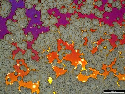
Microscope photograph of WSe2-samples, connected to electrodes
TU Wien
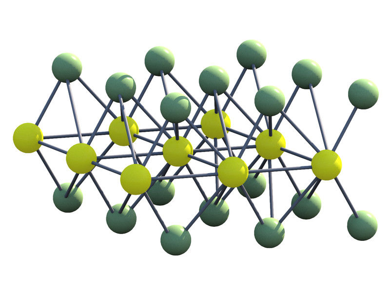
Tungsten diselenide
TU Wien


Thin layers are different
At least since the Nobel Prize in physics was awarded in 2010 for creating graphene, the “two dimensional crystals" made of carbon atoms have been regarded as one of the most promising materials in electronics. In 2013, graphene research was chosen by the EU as a flagship-project, with a funding of one billion euros. Graphene can sustain extreme mechanical strain and it has great opto-electronic properties. With graphene as a light detector, optical signals can be transformed into electric pulses on extremely short timescales.
For one very similar application, however, graphene is not well suited for building solar cells. “The electronic states in graphene are not very practical for creating photovoltaics”, says Thomas Mueller. Therefore, he and his team started to look for other materials, which, similarly to graphene, can arranged in ultrathin layers, but have even better electronic properties.
The material of choice was tungsten diselenide: It consists of one layer of tungsten atoms, which are connected by selenium atoms above and below the tungsten plane. The material absorbs light, much like graphene, but in tungsten diselenide, this light can be used to create electrical power.
The world’s thinnest solar cells
The layer is so thin that 95% of the light just passes through – but a tenth of the remaining five percent, which are absorbed by the material, are converted into electrical power. Therefore, the internal efficiency is quite high. A larger portion of the incident light can be used if several of the ultrathin layers are stacked on top of each other – but sometimes the high transparency can be a useful side effect. “We are envisioning solar cell layers on glass facades, which let part of the light into the building while at the same time creating electricity”, says Thomas Mueller.
Today, standard solar cells are mostly made of silicon, they are rather bulky and inflexible. Organic materials are also used for opto-electronic applications, but they age rather quickly. “A big advantage of two-dimensional structures of single atomic layers is their crystallinity. Crystal structures lend stability”, says Thomas Mueller.
The results of the experiments at the Vienna University of Technology have now been published in the journal “Nature Nanotechnology”. The research field is extremely competitive: in the same issue of the journal, two more papers are published, in which very similar results are shown. Researchers at the MIT (Cambridge, USA) and at the University of Washington (Seattle, USA) have also discovered the great advantages of tungsten diselenide. There seems to be little doubt that this material will soon play an important role in materials science all over the world, much like graphene has in the last couple of years.
Topics
Organizations
Other news from the department science

Get the chemical industry in your inbox
By submitting this form you agree that LUMITOS AG will send you the newsletter(s) selected above by email. Your data will not be passed on to third parties. Your data will be stored and processed in accordance with our data protection regulations. LUMITOS may contact you by email for the purpose of advertising or market and opinion surveys. You can revoke your consent at any time without giving reasons to LUMITOS AG, Ernst-Augustin-Str. 2, 12489 Berlin, Germany or by e-mail at revoke@lumitos.com with effect for the future. In addition, each email contains a link to unsubscribe from the corresponding newsletter.
Most read news
More news from our other portals
Last viewed contents
Novec_1230
Light at the end of the nanotunnel for future catalysts
Leopold_Heinrich_Fischer
Gonadotropin-releasing_hormone
Melanocortin_1_receptor
George_N._Hatsopoulos
Bacillus_Calmette-Guérin
Entecavir
TSKgel HXL Columns | SEC columns | Tosoh
Platelets instead of spheres make screens more economical
Category:Apolipoproteins
