Breakthrough for solar cell efficiency
New atomic layer-by-layer InGaN technology offers perfect crystal
Did you know that Crystals form the basis for the penetrating icy blue glare of car headlights and could be fundamental to the future in solar energy technology?

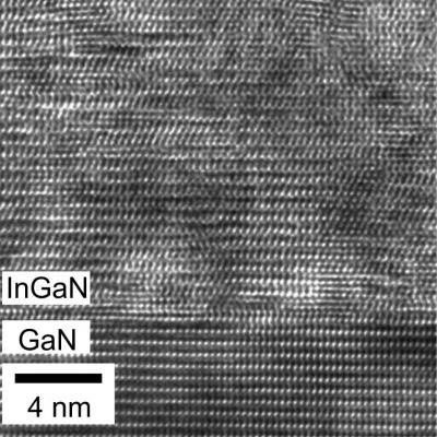
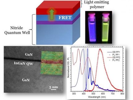
The atomic arrangement at a relaxed InGaN/GaN interface created by layer-by-layer atomic crystal growth is shown. The technique may point to new developments in solar cell efficiency.
Arizona State University
Crystals are at the heart of diodes. Not the kind you might find in quartz, formed naturally, but manufactured to form alloys, such as indium gallium nitride or InGaN. This alloy forms the light emitting region of LEDs, for illumination in the visible range, and of laser diodes (LDs) in the blue-UV range.
Research into making better crystals, with high crystalline quality, light emission efficiency and luminosity, is also at the heart of studies being done at Arizona State University by Research Scientist Alec Fischer and Doctoral Candidate Yong Wei in Professor Fernando Ponce's group in the Department of Physics.
In an article recently published in the journal Applied Physics Letters, the ASU group, in collaboration with a scientific team led by Professor Alan Doolittle at the Georgia Institute of Technology, has just revealed the fundamental aspect of a new approach to growing InGaN crystals for diodes, which promises to move photovoltaic solar cell technology toward record-breaking efficiencies.
The InGaN crystals are grown as layers in a sandwich-like arrangement on sapphire substrates. Typically, researchers have found that the atomic separation of the layers varies; a condition that can lead to high levels of strain, breakdowns in growth, and fluctuations in the alloy's chemical composition.
"Being able to ease the strain and increase the uniformity in the composition of InGaN is very desirable," says Ponce, "but difficult to achieve. Growth of these layers is similar to trying to smoothly fit together two honeycombs with different cell sizes, where size difference disrupts a periodic arrangement of the cells."
As outlined in their publication, the authors developed an approach where pulses of molecules were introduced to achieve the desired alloy composition. The method, developed by Doolittle, is called metal-modulated epitaxy. "This technique allows an atomic layer-by-layer growth of the material," says Ponce.
Analysis of the atomic arrangement and the luminosity at the nanoscale level was performed by Fischer, the lead author of the study, and Wei. Their results showed that the films grown with the epitaxy technique had almost ideal characteristics and revealed that the unexpected results came from the strain relaxation at the first atomic layer of crystal growth.
"Doolittle's group was able to assemble a final crystal that is more uniform and whose lattice structures match up…resulting in a film that resembles a perfect crystal," says Ponce. "The luminosity was also like that of a perfect crystal. Something that no one in our field thought was possible."
The ASU and Georgia Tech team's elimination of these two seemingly insurmountable defects (non-uniform composition and mismatched lattice alignment) ultimately means that LEDs and solar photovoltaic products can now be developed that have much higher, efficient performance.
"While we are still a ways off from record-setting solar cells, this breakthrough could have immediate and lasting impact on light emitting devices and could potentially make the second most abundant semiconductor family, III-Nitrides, a real player in the solar cell field," says Doolittle. Doolittle's team at Georgia Tech's School of Electrical and Computer Engineering also included Michael Moseley and Brendan Gunning. A patent is pending for the new technology.
Other news from the department science

Get the chemical industry in your inbox
By submitting this form you agree that LUMITOS AG will send you the newsletter(s) selected above by email. Your data will not be passed on to third parties. Your data will be stored and processed in accordance with our data protection regulations. LUMITOS may contact you by email for the purpose of advertising or market and opinion surveys. You can revoke your consent at any time without giving reasons to LUMITOS AG, Ernst-Augustin-Str. 2, 12489 Berlin, Germany or by e-mail at revoke@lumitos.com with effect for the future. In addition, each email contains a link to unsubscribe from the corresponding newsletter.


