Major leap towards graphene for solar cells
graphene has extreme conductivity and is completely transparent while being inexpensive and nontoxic. This makes it a perfect candidate material for transparent contact layers for use in solar cells to conduct electricity without reducing the amount of incoming light - at least in theory. Whether or not this holds true in a real world setting is questionable as there is no such thing as "ideal" graphene - a free floating, flat honeycomb structure consisting of a single layer of carbon atoms: interactions with adjacent layers can change graphene's properties dramatically.

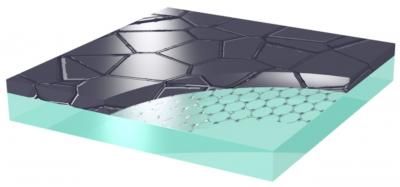
Graphene was deposited onto a glass substrate. The ultrathin layer is but one atomic layer thick (0.3 Angström, or 0.03 nanometers), although charge carriers are able to move about freely within this layer. This property is retained even if the graphene layer is covered with amorphous or polycrystalline silicon.
Marc A. Gluba/HZB
"We examined how graphene's conductive properties change if it is incorporated into a stack of layers similar to a silicon based thin film solar cell and were surprised to find that these properties actually change very little," Marc Gluba explains. To this end, they grew graphene on a thin copper sheet, next transferred it to a glass substrate, and finally coated it with a thin film of silicon. They examined two different versions that are commonly used in conventional silicon thin-film technologies: one sample contained an amorphous silicon layer, in which the silicon atoms are in a disordered state similar to a hardened molten glas; the other sample contained poly-crystalline silicon to help them observe the effects of a standard crystallization process on graphene's properties.
Even though the morphology of the top layer changed completely as a result of being heated to a temperature of several hundred degrees C, the graphene is still detectable. "That's something we didn't expect to find, but our results demonstrate that graphene remains graphene even if it is coated with silicon," says Norbert Nickel.
Their measurements of carrier mobility using the Hall-effect showed that the mobility of charge carriers within the embedded graphene layer is roughly 30 times greater than that of conventional zinc oxide based contact layers. Says Gluba: "Admittedly, it's been a real challenge connecting this thin contact layer, which is but one atomic layer thick, to external contacts. We're still having to work on that." Adds Nickel: "Our thin film technology colleagues are already pricking up their ears and wanting to incorporate it." The researchers obtained their measurements on one square centimeter samples, although in practice it is feasible to coat much larger areas than that with graphene.
Other news from the department science

Get the chemical industry in your inbox
By submitting this form you agree that LUMITOS AG will send you the newsletter(s) selected above by email. Your data will not be passed on to third parties. Your data will be stored and processed in accordance with our data protection regulations. LUMITOS may contact you by email for the purpose of advertising or market and opinion surveys. You can revoke your consent at any time without giving reasons to LUMITOS AG, Ernst-Augustin-Str. 2, 12489 Berlin, Germany or by e-mail at revoke@lumitos.com with effect for the future. In addition, each email contains a link to unsubscribe from the corresponding newsletter.


