Superconducting wire yields unprecedented performance
The ability to control nanoscale imperfections in superconducting wires results in materials with unparalleled and customized performance, according to a new study from the Department of Energy’s Oak Ridge National Laboratory.
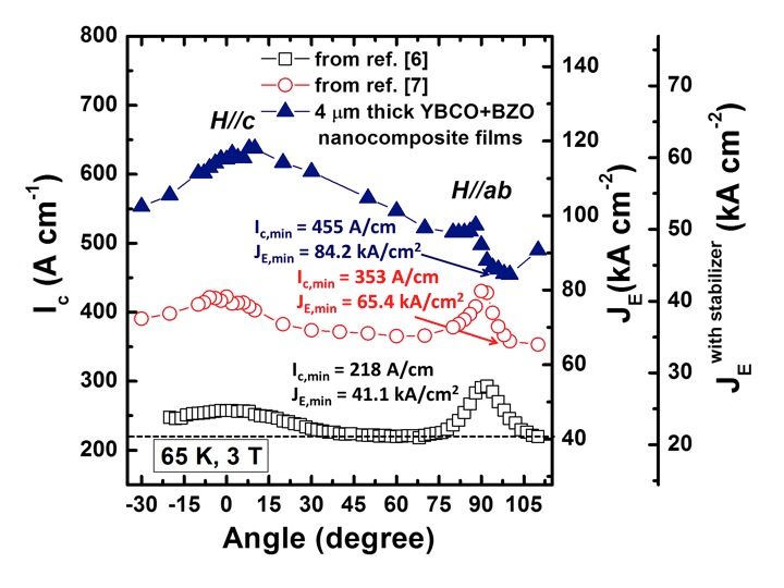
This figure shows the critical current, Ic, and engineering critical current density, JE, in a superconducting wire as a function of applied magnetic field orientation at 65 Kelvin and 3 Tesla. The top curve shows results from a newly published ORNL study. The other two curves are from previously reported record values. A minimum JE of 43.7 kiloamperes/cm2 (assuming a 50 micron thick stabilizer layer) and a minimum Ic of 455 Amperes/cm was obtained for all applied field orientations. This is the highest reported performance for a superconductor wire or a film on a technical substrate.
hi-res image
Applications for superconducting wires, which carry electricity without resistance when cooled to a critical temperature, include underground transmission cables, transformers and large-scale motors and generators. But these applications require wires to operate under different temperature and magnetic field regimes.
A team led by ORNL’s Amit Goyal demonstrated that superconducting wires can be tuned to match different operating conditions by introducing small amounts of non-superconducting material that influences how the overall material behaves. Manipulating these nanoscale columns -- also known as defects -- allows researchers to exert control over the forces that regulate the wires’ superconducting performance. The team’s findings are published in Nature Publishing Group’s Scientific Reports.
“Not only can we introduce these nanocolumn defects within the superconductor and get enhanced performance, but we can optimize the performance for different application regimes by modifying the defect spacing and density,” Goyal said.
A wire sample grown with this process exhibited unprecedented performance in terms of engineering critical current density, which measures the amount of current the wire can carry per unit cross-sectional area. This metric more accurately reflects the real-world capabilities of the material because it takes into account the wire’s non-superconducting components such as the substrate and the buffer and stabilizer layers, Goyal said.
“We report a record performance at 65 Kelvin and 3 Tesla, where most rotating machinery applications like motors and generators are slated to operate,” he said.
The paper reports a minimum engineering critical current density at all applied magnetic field orientations of 43.7 kiloamperes/cm2, which is more than twice the performance level needed for most applications. This metric assumes the presence of a 50-micron-thick copper stabilizer layer required in applications.
Generating defects in the superconductor is accomplished through an ORNL-developed self-assembly process, which enables researchers to design a material that automatically develops the desired nanoscale microstructure during growth.
The mechanism behind this process, which adds very little to the production cost, was the subject of a recently published study by a team led by Goyal in Advanced Functional Materials.
“When you’re making the wires, you can dial-in the properties because the defects self-assemble,” Goyal said. “You change the composition of the superconductor when you’re depositing the tape.”
Goyal, who has collaborated with multiple superconducting technology companies, hopes the private sector will incorporate the team’s findings to improve upon existing products and generate new applications.
Other news from the department science