Spot-welding graphene nanoribbons atom by atom
Scientists at Aalto University, Finland and Utrecht University, the Netherlands have created single atom contacts between gold and graphene nanoribbons.
In their article published in Nature Communications, the research team demonstrates how to make electrical contacts with single chemical bonds to graphene nanoribbons. Graphene is a single layer of carbon atoms arranged in a honeycomb lattice. It is anticipated to be a revolutionising material for future electronics.
Graphene transistors functioning at room temperature require working at the size scale of less than 10 nanometres. This means that the graphene nanostructures have to be only a few tens of atoms in width. These transistors will need atomically precise electrical contacts. A team of researchers have now demonstrated experimentally how this can be done.
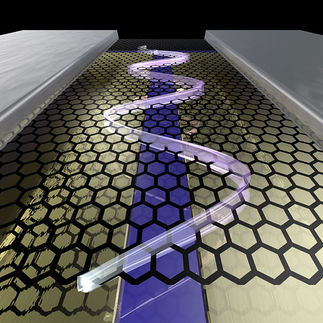
In their article the scientists address the problem by demonstrating how a single chemical bond can be used to make an electrical contact to a graphene nanoribbon.
"We cannot use alligator clips on the atomic scale. Using well-defined chemical bonds is the way forward for graphene nanostructures to realise their potential in future electronics", says Professor Peter Liljeroth who heads the Atomic Scale Physics group at Aalto University.
The team used atomic force microscopy (AFM) and scanning tunnelling microscopy (STM) to map the structure of the graphene nanoribbons with atomic resolution. The researchers used voltage pulses from the tip of the scanning tunnelling microscope to form single bonds to the graphene nanoribbons – precisely at a specific atomic location. The pulse removes a single hydrogen atom from the end of a graphene nanoribbon and this initiates the bond formation.
"Combined AFM and STM allows us to characterise the graphene nanostructures atom-by-atom, which is critical in understanding how the structure, the bonds with the contacts and their electrical properties are related", explains Dr Ingmar Swart who leads the team concentrating on STM and AFM measurements at Utrecht University.
Combining the microscopy experiments with theoretical modelling, the team developed a detailed picture of the contacted nanoribbon properties. The most significant discovery is that a single chemical bond forms an electronically transparent contact with the graphene nanoribbon – without affecting its overall electronic structure. This may be the key to using graphene nanostructures in future electronic devices, as the contact does not change the intrinsic ribbon properties.
"These experiments on atomically well-defined structures allow us to quantitatively compare theory and experiment. This is a great opportunity to test novel theoretical ideas", concludes Dr Ari Harju, leader of the theoretical team in the project at Aalto University.
Topics
Organizations
Other news from the department science

Get the chemical industry in your inbox
By submitting this form you agree that LUMITOS AG will send you the newsletter(s) selected above by email. Your data will not be passed on to third parties. Your data will be stored and processed in accordance with our data protection regulations. LUMITOS may contact you by email for the purpose of advertising or market and opinion surveys. You can revoke your consent at any time without giving reasons to LUMITOS AG, Ernst-Augustin-Str. 2, 12489 Berlin, Germany or by e-mail at revoke@lumitos.com with effect for the future. In addition, each email contains a link to unsubscribe from the corresponding newsletter.


