Nanowires grown on graphene have surprising structure
When a team of University of Illinois engineers set out to grow nanowires of a compound semiconductor on top of a sheet of graphene, they did not expect to discover a new paradigm of epitaxy.

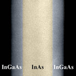
A false-color microscope image of a single nanowire, showing the InAs core and InGaAs shell.
Parsian Mohseni
The self-assembled wires have a core of one composition and an outer layer of another, a desired trait for many advanced electronics applications. Led by professor Xiuling Li, in collaboration with professors Eric Pop and Joseph Lyding, all professors of electrical and computer engineering, the team published its findings in the journal Nano Letters.
Nanowires, tiny strings of semiconductor material, have great potential for applications in transistors, solar cells, lasers, sensors and more.
“Nanowires are really the major building blocks of future nano-devices,” said postdoctoral researcher Parsian Mohseni, first author of the study. “Nanowires are components that can be used, based on what material you grow them out of, for any functional electronics application.”
Li’s group uses a method called van der Waals epitaxy to grow nanowires from the bottom up on a flat substrate of semiconductor materials, such as silicon. The nanowires are made of a class of materials called III-V (three-five), compound semiconductors that hold particular promise for applications involving light, such as solar cells or lasers.
The group previously reported growing III-V nanowires on silicon. While silicon is the most widely used material in devices, it has a number of shortcomings. Now, the group has grown nanowires of the material indium gallium arsenide (InGaAs) on a sheet of graphene, a 1-atom-thick sheet of carbon with exceptional physical and conductive properties.
Thanks to its thinness, graphene is flexible, while silicon is rigid and brittle. It also conducts like a metal, allowing for direct electrical contact to the nanowires. Furthermore, it is inexpensive, flaked off from a block of graphite or grown from carbon gases.
“One of the reasons we want to grow on graphene is to stay away from thick and expensive substrates,” Mohseni said. “About 80 percent of the manufacturing cost of a conventional solar cell comes from the substrate itself. We’ve done away with that by just using graphene. Not only are there inherent cost benefits, we’re also introducing functionality that a typical substrate doesn’t have.”
The researchers pump gases containing gallium, indium and arsenic into a chamber with a graphene sheet. The nanowires self-assemble, growing by themselves into a dense carpet of vertical wires across the surface of the graphene. Other groups have grown nanowires on graphene with compound semiconductors that only have two elements, but by using three elements, the Illinois group made a unique finding: The InGaAs wires grown on graphene spontaneously segregate into an indium arsenide (InAs) core with an InGaAs shell around the outside of the wire.
“This is unexpected,” Li said. “A lot of devices require a core-shell architecture. Normally you grow the core in one growth condition and change conditions to grow the shell on the outside. This is spontaneous, done in one step. The other good thing is that since it’s a spontaneous segregation, it produces a perfect interface.”
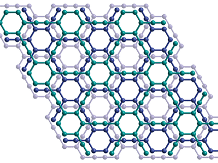
So what causes this spontaneous core-shell structure? By coincidence, the distance between atoms in a crystal of InAs is nearly the same as the distance between whole numbers of carbon atoms in a sheet of graphene. So, when the gases are piped into the chamber and the material begins to crystallize, InAs settles into place on the graphene, a near-perfect fit, while the gallium compound settles on the outside of the wires. This was unexpected, because normally, with van der Waals epitaxy, the respective crystal structures of the material and the substrate are not supposed to matter.
“We didn’t expect it, but once we saw it, it made sense,” Mohseni said.
In addition, by tuning the ratio of gallium to indium in the semiconductor cocktail, the researchers can tune the optical and conductive properties of the nanowires.
Next, Li’s group plans to make solar cells and other optoelectronic devices with their graphene-grown nanowires. Thanks to both the wires’ ternary composition and graphene’s flexibility and conductivity, Li hopes to integrate the wires in a broad spectrum of applications.
“We basically discovered a new phenomenon that confirms that registry does count in van der Waals epitaxy,” Li said.


