Magnetic fingerprints of interface defects in silicon solar cells detected
Advertisement


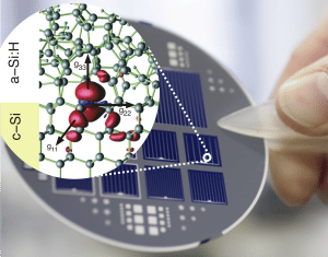
In theory, silicon-based solar cells are capable of converting up to 30 percent of sunlight to electricity - although, in reality, the different kinds of loss mechanisms ensure that even under ideal lab conditions it does not exceed 25 %. Advanced heterojunction cells shall affront this problem: On top of the wafer's surface, at temperatures below 200 °C, a layer of 10 nanometer disordered (amorphous) silicon is deposited. This thin film is managing to saturate to a large extent the interface defects and to conduct charge carriers out of the cell. Heterojunction solar cells have already high efficiency factors up to 24,7 % – even in industrial scale. However, scientists had until now only a rough understanding of the processes at the remaining interface defects.
Magnetic fingerprints of interface defects in silicon solar cells detected.
HZB / University Paderborn
Now, physicists at HZB's Institute for Silicon Photovoltaics have figured out a rather clever way for detecting the remaining defects and characterizing their electronic structure. "If electrons get deposited on these defects, we are able to use their spin, that is, their small magnetic moment, as a probe to study them," Dr. Alexander Schnegg explains. With the help of EDMR, electrically detected magnetic resonance, an ultrasensitive method of measurement, they were able to determine the local defects' structure by detecting their magnetic fingerprint in the photo current of the solar cell under a magnetic field and microwave radiation.
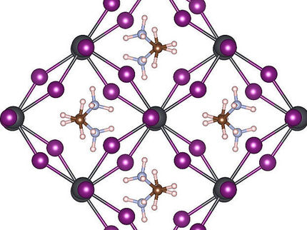
Theoretical physicists of Paderborn University could compare these results with quantum chemical computer simulations, thus obtaining information about the defects' positions within the layers and the processes they are involved to decrease the cells' efficiency. "We basically found two distinct families of defects", says Dr. Uwe Gerstmann from Paderborn University, who collaborates with the HZB Team in a program sponsored by Deutsche Forschungsgemeinschaft (DFG priority program 1601). "Whereas in the first one, the defects are rather weakly localized within the amorphous layer, a second family of defects is found directly at the interface, but in the crystalline silicon."
For the first time ever the scientists have succeeded at directly detecting and characterizing processes with atomic resolution that compromise these solar cells' high efficiency. The cells were manufactured and measured at the HZB; the numerical methods were developed at Paderborn University. "We can now apply these findings to other types of solar cells in order to optimize them further and to decrease production costs", says Schnegg.


Other news from the department science


