Low-resistance connections facilitate multi-walled carbon nanotubes for interconnects
Using a new method for precisely controlling the deposition of carbon, researchers have demonstrated a technique for connecting multi-walled carbon nanotubes to the metallic pads of integrated circuits without the high interface resistance produced by traditional fabrication techniques.
Based on electron beam-induced deposition (EBID), the work is believed to be the first to connect multiple shells of a multi-walled carbon nanotube to metal terminals on a semiconducting substrate, which is relevant to integrated circuit fabrication. Using this three-dimensional fabrication technique, researchers at the Georgia Institute of Technology developed graphitic nanojoints on both ends of the multi-walled carbon nanotubes, which yielded a 10-fold decrease in resistivity in its connection to metal junctions.
The technique could facilitate the integration of carbon nanotubes as interconnects in next-generation integrated circuits that use both silicon and carbon components. The research was supported by the Semiconductor Research Corporation, and in its early stages, by the National Science Foundation. The work was reported by IEEE Transactions on Nanotechnology.
"For the first time, we have established connections to multiple shells of carbon nanotubes with a technique that is amenable to integration with conventional integrated circuit microfabrication processes," said Andrei Fedorov, a professor in the George W. Woodruff School of Mechanical Engineering at Georgia Tech. "Connecting to multiple shells allows us to dramatically reduce the resistance and move to the next level of device performance."
In developing the new technique, the researchers relied on modeling to guide their process parameters. To make it scalable for manufacturing, they also worked toward technologies for isolating and aligning individual carbon nanotubes between the metal terminals on a silicon substrate, and for examining the properties of the resulting structures. The researchers believe the technique could also be used to connect multi-layered graphene to metal contacts, though their published research has so far focused on carbon nanotubes.
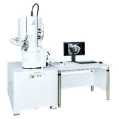
The low-temperature EBID process takes place in a scanning electron microscope (SEM) system modified for material deposition. The SEM's vacuum chamber is altered to introduce precursors of the materials that researchers would like to deposit. The electron gun normally used for imaging of nanostructures is instead used to generate low energy secondary electrons when the high energy primary electrons impinge on the substrate at carefully chosen locations. When the secondary electrons interact with hydrocarbon precursor molecules introduced into the SEM chamber, carbon is deposited in desired locations.
Unique to the EBID process, the deposited carbon makes a strong, chemically-bonded connection to the ends of the carbon nanotubes, unlike the weakly-coupled physical interface made in traditional techniques based on metal evaporation. Prior to deposition, the ends of the nanotubes are opened using an etching process, so the deposited carbon grows into the open end of the nanotube to electronically connect multiple shells. Thermal annealing of the carbon after deposition converts it to a crystalline graphitic form that significantly improves electrical conductivity.
"Atom-by-atom, we can build the connection where the electron beam strikes right near the open end of the carbon nanotubes," Fedorov explained. "The highest rate of deposition occurs where the concentration of precursor is high and there are a lot of secondary electrons. This provides a nanoscale sculpturing tool with three-dimensional control for connecting the open ends of carbon nanotubes on any desired substrate."
Multi-walled carbon nanotubes offer the promise of higher information delivery throughput for certain interconnects used in electronic devices. Researchers have envisioned a future generation of hybrid devices based on traditional integrated circuits but using interconnects based on carbon nanotubes.
Until now, however, resistance at the connections between the carbon structures and conventional silicon electronics has been too high to make the devices practical.
"The big challenge in this field is to make a connection not just to a single shell of a carbon nanotube," said Fedorov. "If only the outer wall of a carbon nanotube is connected, you really don't gain much because most of the transmission channel is under-utilized or not utilized at all."
The technique developed by Fedorov and his collaborators produces record low resistivity at the connection between the carbon nanotube and the metal pad. The researchers have measured resistance as low as approximately 100 Ohms – a factor of ten lower than the best that had been measured with other connection techniques.
"This technique gives us many new opportunities to go forward with integrating these carbon nanostructures into conventional devices," he said. "Because it is carbon, this interface has an advantage because its properties are similar to those of the carbon nanotubes to which they are providing a connection."
The researchers don't know exactly how many of the carbon nanotube shells are connected, but based on resistance measurements, they believe at least 10 of the approximately 30 conducting shells are contributing to electrical conduction.
However, handling carbon nanotubes poses a significant challenge to their use as interconnects. When formed through the electric arc technique, for example, carbon nanotubes are produced as a tangle of structures with varying lengths and properties, some with mechanical defects. Techniques have been developed to separate out single nanotubes, and to open their ends.
Fedorov and his collaborators – current and former graduate students Songkil Kim, Dhaval Kulkarni, Konrad Rykaczewski and Mathias Henry, along with Georgia Tech professor Vladimir Tsukruk – developed a method for aligning the multi-walled nanotubes across electronic contacts using focused electrical fields in combination with a substrate template created through electron beam lithography. The process has a significantly improved yield of properly aligned carbon nanotubes, with a potential for scalability over a large chip area.
Once the nanotubes are placed into their positions, the carbon is deposited using the EBID process, followed by graphitization. The phase transformation in the carbon interface is monitored using Raman spectroscopy to ensure that the material is transformed into its optimal nanocrystalline graphite state.
"Only by making advances in each of these areas can we achieve this technological advance, which is an enabling technology for nanoelectronics based on carbon materials," he said. "This is really a critical step for making many different kinds of devices using carbon nanotubes or graphene."
Before the new technique can be used on a large scale, researchers will have to improve their technique for aligning carbon nanotubes and develop EBID systems able to deposit connectors on multiple devices simultaneously. Advances in parallel electron beam systems may provide a way to mass-produce the connections, Fedorov said.
"A major amount of work remains to be done in this area, but we believe this is possible if industry becomes interested," he noted. "There are applications where integrating carbon nanotubes into circuits could be very attractive."


