New technique controls crystalline structure of titanium dioxide
Researchers from North Carolina State University have developed a new technique for controlling the crystalline structure of titanium dioxide at room temperature. The development should make titanium dioxide more efficient in a range of applications, including photovoltaic cells, hydrogen production, antimicrobial coatings, smart sensors and optical communication technologies.

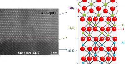
A new technique allows researchers to control the phase of the titanium dioxide by modifying the structure of the titanium trioxide and sapphire substrate.
Dr. Jay Narayan, North Carolina State University
Titanium dioxide most commonly comes in one on of two major "phases," meaning that its atoms arrange themselves in one of two crystalline structures. These phases are "anatase" or "rutile." The arrangement of atoms dictates the material's optical, chemical and electronic properties. As a result, each phase has different characteristics. The anatase phase has characteristics that make it better suited for use as an antibacterial agent and for applications such as hydrogen production. The rutile phase is better suited for use in other applications, such as photovoltaic cells, smart sensors and optical communication technologies.
"Traditionally, it has been a challenge to stabilize titanium dioxide in the desired phase," says Dr. Jay Narayan, John C. Fan Distinguished Chair Professor of Materials Science and Engineering at NC State and co-author of a paper describing the work. "The material tends to transform into the anatase phase below 500 degrees Celsius [C], and transform into the rutile phase at temperatures above 500 C.
"We have now developed a technique that precisely controls the phase, or crystalline structure, of titanium dioxide at room temperature – and stabilizes that phase, so it won't change when the temperature fluctuates. This process, called phase tuning, allows us to fine-tune the structure of the titanium dioxide, so that it has the optimal structure for a desired application."
The process begins by using a widely available sapphire substrate that has the desired crystalline structure. Researchers then grow a template layer of titanium trioxide on the substrate. The structure of the titanium trioxide mimics the structure of the sapphire substrate. The titanium dioxide is then grown on top of the titanium trioxide template layer.
The structure of the titanium dioxide differs from the titanium trioxide – but is dictated by the structure of that template layer. This means that you can create the titanium dioxide in any phase, simply by modifying the structure of the titanium trioxide and sapphire substrate.
This works because of a process called domain matching epitaxy (DME). In DME, the lattice planes in the template layer line up with the lattice planes of the material being grown on that template. Lattice planes are the lines, or walls, which constitute a crystal.
The researchers have also demonstrated how this technique can be used with silicon computer chip substrates, which can be integrated into electronics such as smart sensors.
Original publication
Domain epitaxy in TiO2/[alpha]-Al2O3 thin film heterostructures with Ti2O3 transient layer; Applied Physics Letters
Original publication
Domain epitaxy in TiO2/[alpha]-Al2O3 thin film heterostructures with Ti2O3 transient layer; Applied Physics Letters
Other news from the department science

Get the chemical industry in your inbox
By submitting this form you agree that LUMITOS AG will send you the newsletter(s) selected above by email. Your data will not be passed on to third parties. Your data will be stored and processed in accordance with our data protection regulations. LUMITOS may contact you by email for the purpose of advertising or market and opinion surveys. You can revoke your consent at any time without giving reasons to LUMITOS AG, Ernst-Augustin-Str. 2, 12489 Berlin, Germany or by e-mail at revoke@lumitos.com with effect for the future. In addition, each email contains a link to unsubscribe from the corresponding newsletter.


