Researchers capture first images of sub-nano pore structures
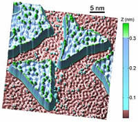
Moore's law marches on: In the quest for faster and cheaper computers, scientists have imaged pore structures in insulation material at sub-nanometer scale for the first time. Understanding these structures could substantially enhance computer performance and power usage of integrated circuits, say Semiconductor Research Corporation (SRC) and Cornell University scientists.
To help maintain the ever-increasing power and performance benefits of semiconductors – like the speed and memory trend described in Moore's law – the industry has introduced very porous, low-dielectric constant materials to replace silicon dioxide as the insulator between nano-scaled copper wires. This has sped up the electrical signals sent along these copper wires inside a computer chip, and at the same time reduced power consumption.
"Knowing how many of the molecule-sized voids in the carefully-engineered Swiss cheese survive in an actual device will greatly affect future designs of integrated circuits," said David Muller, Cornell University professor of applied and engineering physics, and co-director of Kavli Institute for Nanoscale Science at Cornell. "The techniques we developed look deeply, as well as in and around the structures, to give a much clearer picture so complex processing and integration issues can be addressed."
The scientists understand that the detailed structure and connectivity of these nanopores have profound control on the mechanical strength, chemical stability and reliability of these dielectrics. With today's announcement, researches now have a nearly atomic understanding of the three-dimensional pore structures of low-k materials required to solve these problems.
Welcome to the atomic world: SRC and Cornell researchers were able to devise a method to obtain 3-D images of the pores using electron tomography, leverages imaging advances used for CT scans and MRIs in the medical field, says Scott List, director of interconnect and packaging sciences at SRC, at Research Triangle Park, N.C. "Sophisticated software extracts 3-D images from a series of 2-D images taken at multiple angles. A 2-D picture is worth a thousand words, but a 3-D image at near atomic resolution gives the semiconductor industry new insights into scaling low-k materials for several additional technology nodes."
Most read news
Other news from the department science
These products might interest you

Limsophy by AAC Infotray
Optimise your laboratory processes with Limsophy LIMS
Seamless integration and process optimisation in laboratory data management

LAUDA.LIVE by LAUDA
LAUDA.LIVE - The digital platform for your device management
Comprehensive fleet management options for every LAUDA device - with and without IoT connectivity
ZEISS ZEN core by Carl Zeiss
ZEISS ZEN core - Your Software suite for connected microscopy in laboratory and production
The comprehensive solution for imaging, segmentation, data storage and analysis

ERP-Software GUS-OS Suite by GUS
Holistic ERP solution for companies in the process industry
Integrate all departments for seamless collaboration

Get the chemical industry in your inbox
By submitting this form you agree that LUMITOS AG will send you the newsletter(s) selected above by email. Your data will not be passed on to third parties. Your data will be stored and processed in accordance with our data protection regulations. LUMITOS may contact you by email for the purpose of advertising or market and opinion surveys. You can revoke your consent at any time without giving reasons to LUMITOS AG, Ernst-Augustin-Str. 2, 12489 Berlin, Germany or by e-mail at revoke@lumitos.com with effect for the future. In addition, each email contains a link to unsubscribe from the corresponding newsletter.
