Improved analysis of silicon surfaces
Progress for photovoltaics, for example

A new method for analyzing rough silicon surfaces combines atomic force microscopy (AFM) and X-ray photoelectron spectroscopy (XPS). This makes it easier to correct errors caused by surface roughness. The method delivers more precise results, particularly with black silicon, a special, nanostructured silicon surface that is frequently used in photovoltaics. These developments are significant for the research and application of nanostructured materials. The work was published in the journal Small Methods.

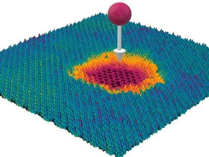
Schematic diagram; yellow: X-ray light leads to the emission of photoelectrons (red). The detector registers the photoelectrons, which originate either from the Si or the Si oxide layer, perpendicular to the smooth surface (left).
Frank Müller, AG Jacobs
The combination of atomic force microscopy (AFM) and X-ray photoelectron spectroscopy (XPS) represents a significant advance in surface characterization. XPS is an established method for determining the chemical composition of surfaces. However, for rough surfaces such as black silicone, XPS analysis is distorted by the different emission angles of the photoelectrons (see figure), which can lead to a strong overestimation of the true layer thicknesses. On the smooth surface (left) the photoelectron is emitted perpendicular to the surface and the oxide layer, whereas on the rough surface (right) the surface inclination relative to the detector leads to a longer path of the photoelectron through the oxide. The resulting XPS spectra are therefore distorted for rough surfaces, which results in an excessively high oxide layer thickness in the analysis. In order to correct these errors, the team led by Professor Dr. Karin Jacobs in the Department of Physics at Saarland University has developed a method that uses AFM measurements to precisely determine the surface topography and incorporate this information into the analysis of the XPS data.
This method is particularly important for the analysis of black silicon, a special silicon surface that is given a nanostructured, highly rough surface through targeted etching processes. "This roughness reduces light reflection and increases light absorption, which makes black silicon particularly interesting for applications in photovoltaics," explains PD Dr. Frank Müller, the team's XPS expert. The new method now makes it possible to determine the thickness of the oxide layer on black silicon with unprecedented accuracy.
The scientists use a new type of geometric analysis of the topography image of the surface provided by the AFM. "So-called Minkowski tensors make it possible to precisely determine the local inclination of the surface and to incorporate this information from the AFM into the evaluation of the XPS spectra," explains the Saarbrücken team's cooperation partner, Dr. Michael Klatt, theoretical physicist at the German Aerospace Center (DLR) in Ulm and Cologne. "In this way, the distortions caused by the surface roughness are corrected and the oxide layer thickness can be determined much more precisely," explains Jens Uwe Neurohr, who is doing his doctorate in this field.
The results of the study show that the oxide layer on black silicon is only around 50 to 80 percent thicker than the native oxide layer on a conventional silicon wafer. Without the correction by the AFM data, a value of around 300 percent would have been determined, i.e. a massive overestimation of the actual conditions.
This combination of methods is particularly valuable for materials research, as it enables a more precise characterization of surfaces that have complex geometries due to nanostructuring or roughness. "However, this is of great interest not only for photovoltaics, but also for other applications in which the surface texture and chemical properties are of crucial importance," says Karin Jacobs about the fundamental importance of these improvements. "The precise determination of layer thicknesses on nano-rough surfaces is a major challenge. With our new method, we can now overcome this challenge and deliver more precise results, which is of enormous importance, especially for the development of high-tech materials," adds Frank Müller.
The research was carried out as part of the priority program SPP 2265 "Random Geometric Systems" funded by the German Research Foundation (DFG) and the Collaborative Research Centre SFB 1027 and represents an important step in the further development of surface analysis techniques. This progress will not only advance materials science, but also support the development of new technologies in areas such as photovoltaics, optoelectronics and nanotechnology.
Note: This article has been translated using a computer system without human intervention. LUMITOS offers these automatic translations to present a wider range of current news. Since this article has been translated with automatic translation, it is possible that it contains errors in vocabulary, syntax or grammar. The original article in German can be found here.
Original publication
Other news from the department science


These products might interest you

OCA 200 by DataPhysics
Using contact angle meter to comprehensively characterise wetting behaviour, solids, and liquids
With its intuitive software and as a modular system, the OCA 200 answers to all customers’ needs

DCAT by DataPhysics
High precision tensiometer for surface and interface analysis
Modular, extendable, powerful - ideal for laboratory and research
MSA One-Click SFE by KRÜSS
MSA One-Click SFE
Analyzing wettability in a second with only one click

NEXSA by Thermo Fisher Scientific
Fully automated, multi-technique surface analysis system to advance your research
Efficient workflows with XPS, UPS, ISS, REELS and Raman spectroscopy

Most read news


More news from our other portals


See the theme worlds for related content
Topic World Spectroscopy
Investigation with spectroscopy gives us unique insights into the composition and structure of materials. From UV-Vis spectroscopy to infrared and Raman spectroscopy to fluorescence and atomic absorption spectroscopy, spectroscopy offers us a wide range of analytical techniques to precisely characterize substances. Immerse yourself in the fascinating world of spectroscopy!