Rigaku Wins Diana Nyyssonen Memorial Best Paper Award
Non-destructive visualization of nanoscale structures realized using ultra-high-resolution X-ray microscope
Rigaku Corporation, a Group company of Rigaku Holdings Corporation has won the Diana Nyyssonen Memorial Best Paper Award (hereinafter “the Award”) with a revolutionary, non-destructive method of discovering defects in 3D flash memory. The inspection and measurement technology (hereinafter “the Technology”) uses an ultra-high-resolution X-ray microscope.

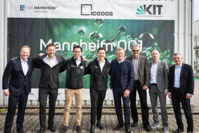
From left: Award recipients Kazuhiko Omote, General Manager, X-ray Research Laboratory; and Raita Hirose, Imaging Group, Advanced Analytical Technology Research Department, X-ray Laboratory
Rigaku
The Award is conferred on the team that delivers the most compelling paper in the fields of measurement, inspection and process control at the SPIE Advanced Lithography + Patterning Conferences. These conferences report the latest research results on lithographic technologies applied in semiconductor manufacturing.
One issue occurring at 3D flash memory production sites is the difficulty of inspecting and measuring the shapes of embedded metal structures and extremely deep holes known as “memory holes."
The technology developed by the Rigaku team achieves ultra-high resolution by employing X-rays, whose detection limit is 1/10 or lower that of the best optical microscopes. In addition to revealing the extremely fine structures of the nanoscale, the technology enables non-destructive observation of devices formed on silicon substrates. The revolutionary nature of this solution is what persuaded the Conferences to confer the award.
Kazuhiko Omote, General Manager of X-ray Research Laboratory, one of the authors of the paper, states that, “By introducing equipment incorporating this technology, 3D flash memory worksites can expect to enjoy improved yields and optimized production processes. Rigaku targets implementation of the technology in this way in about two years’ time“.
Going forward, Rigaku aims to leverage this technology in pursuit of further innovations, such as application in inspection and measurement of conductance in the connective parts of multilayered devices.

Other news from the department business & finance