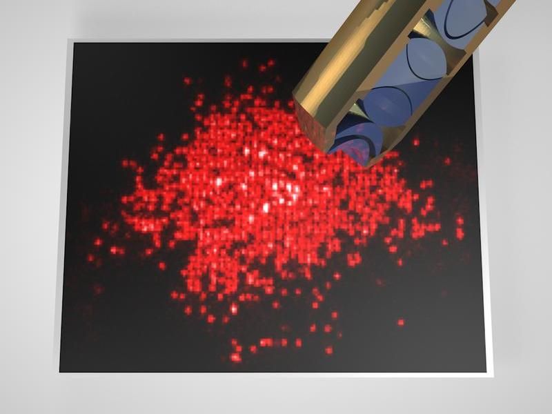
Mesoporous silicon: semiconductor with new talents
Silicon is the best-known semiconductor material. However, targeted nanostructuring can drastically change the material properties. A team at HZB has now produced mesoporous silicon layers with countless tiny pores using a specially developed etching apparatus and investigated their electrical conductivity and thermopower. The researchers have thus elucidated for the first time how electronic transport works in this mesoporous silicon. The material has great potential for applications and could also thermally insulate qubits for quantum computers.
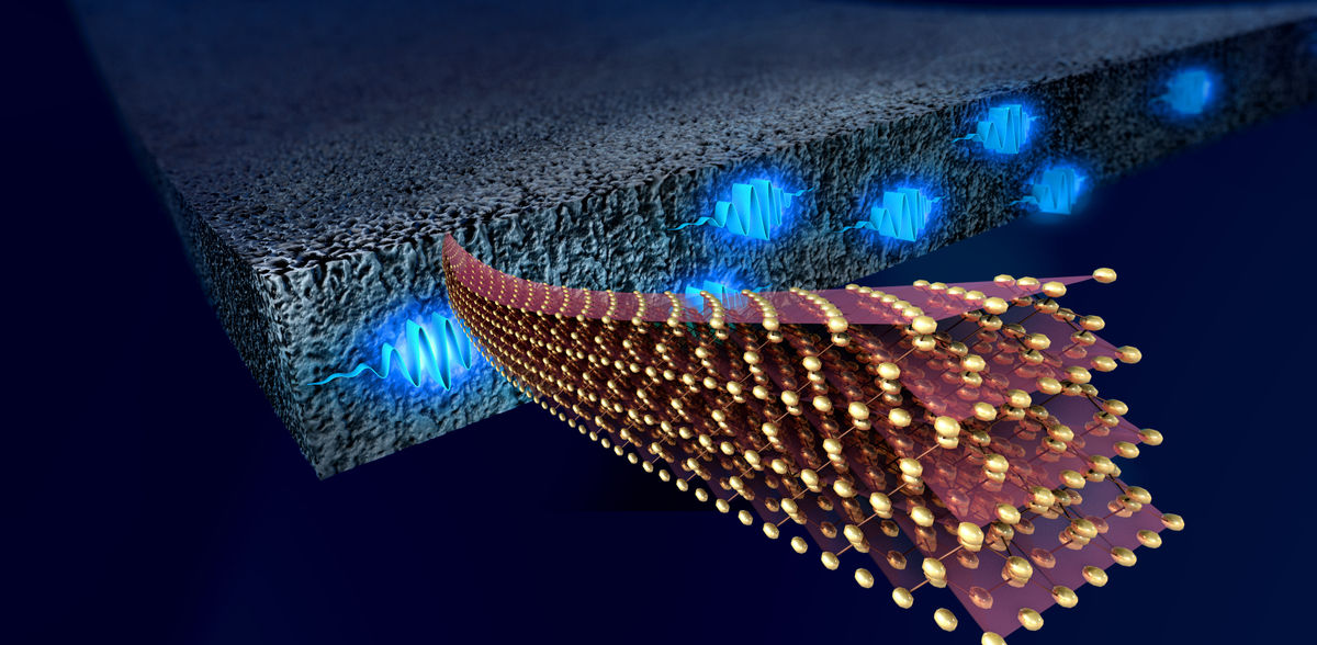
Mesoporous silicon is crystalline silicon with disordered nanometer-sized pores. The material has a huge inner surface area and is also biocompatible. This results in a wide range of application options, from biosensors to battery anodes and capacitors. The material also has exceptionally low thermal conductivity, which is interesting for thermal insulation applications.
What dominates the transport?
Although mesoporous silicon has been known for decades, a fundamental understanding of the transport of charge carriers and the possible involvement of lattice vibrations (phonons) in charge transport in this material has been lacking until now. "Understanding the transport properties and processes precisely is, however, a prerequisite for further developing the material in a targeted manner," says Dr. Klaus Habicht, who heads the Dynamics and Transport in Quantum Materials (QM-ADT) department at HZB.
Habicht and his team have now presented this analysis. They synthesized a series of silicon nanostructures using an etching technique optimized at HZB and determined the temperature-dependent electrical conductivity and thermal force.
Wave-like electron states
"By analysing the measurement data, we were able to clearly identify the fundamental process in charge transport," says Dr. Tommy Hofmann, first author of the study. The key finding: "The charge transport is not dominated by electrons localized by disorder, which hop from one localized state to the next, but by electrons in extended, wave-like states." The conductivity decreases with increasing disorder. The activation energy required to bring charge carriers over a "mobility edge" that depends on the disorder increases.
Lattice vibrations play no role
Unlike in a hopping process, lattice vibrations play no role in charge transport. This was shown in particular by measurements of the Seebeck effect, in which the electrical voltage is determined that arises when the sample is exposed to a temperature difference along a defined direction.
"This is the first time we have provided a reliable and novel explanation for the microscopic charge carrier transport in disordered, nanostructured silicon," explains Dr. Tommy Hofmann.
Mesoporous silicon as insulation for qubits
These results are of practical relevance, as mesoporous silicon could be ideal for silicon-based qubits. These qubits operate in the low temperature range, typically below 1 Kelvin, and require very good thermal insulation to avoid absorbing heat from the environment and erasing the information stored in qubits. "Using a metaphorical comparison, mesoporous silicon could be seen as a kind of insulating foam, like in house construction," says Habicht.
Disorder can be used
The use of mesoporous silicon may also be suitable for semiconductor applications that have so far failed due to the high thermal conductivity of crystalline or polycrystalline silicon. "The disorder can be used in a targeted manner," emphasizes Habicht. Semiconductors with purely stochastically distributed mesopores would therefore be an exciting new class of materials for technical applications ranging from photovoltaics, thermal management and nanoelectronics to qubits for quantum computers.
Note: This article has been translated using a computer system without human intervention. LUMITOS offers these automatic translations to present a wider range of current news. Since this article has been translated with automatic translation, it is possible that it contains errors in vocabulary, syntax or grammar. The original article in German can be found here.

Other news from the department science