Metamaterial for the terahertz age
Tailored quantum materials as a high-efficiency frequency booster
An international research team, comprising scientists from the Helmholtz-Zentrum Dresden-Rossendorf (HZDR), the Catalan Institute of Nanoscience and Nanotechnology and JMU Würzburg, has found a way of generating terahertz radiation by frequency conversion much more efficient than with previous technologies. A specially constructed quantum materials system acts as a high-efficiency frequency booster.
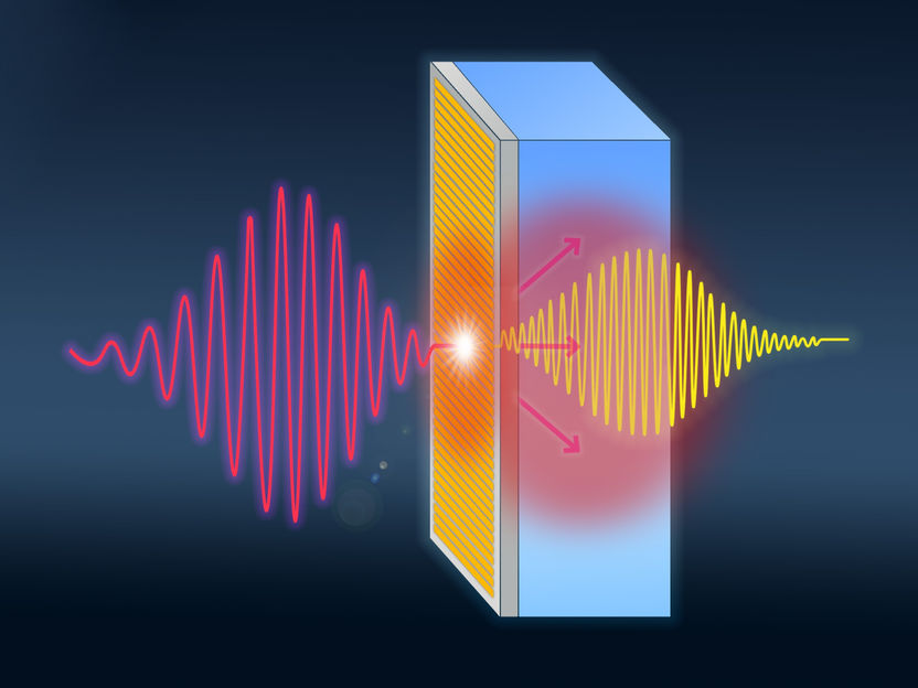
A low-frequency 500 GHz pulse (red) hits the metamaterial: a topological insulator with gold structures. On the surface of the sample new terahertz waves are generated with a multiple of the input frequency (yellow).
© WERKSTATT X / HZDR
Terahertz-waves are high-frequency electromagnetic waves between the microwave and infrared ranges. In the future, they could accelerate optoelectronic applications and supersede today’s gigahertz technologies in communications. With clock rates a thousand times higher, the terahertz range facilitates extremely fast data transfer and could offer a basis for sixth generation mobile communication networks. But before that, there are technical hurdles to be overcome. The terahertz range has yet to be sufficiently researched: suitable components are missing; at present, many systems can only be used in their current form in special labs and in combination with high-performance lasers. Researchers are therefore investigating practice-related solutions.
“The terahertz frequency range is precisely the frontier of ultrafast electronics in which many barely-explored quantum phenomena become relevant. For new optoelectronic components we first have to find out which materials and methods are suitable,” says Dr. Sergey Kovalev, group head at the terahertz facility TELBE in HZDR’s Institute of Radiation Physics, who was responsible for the experiments. The TELBE source is designed for the investigation of new materials and their interactions with intensive terahertz pulses.
Hundred times more power
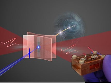
Certain quantum materials are particularly promising as they can be used as a kind of frequency booster to convert electronically generated gigahertz radiation into the neighboring terahertz range. This is achieved by high-efficiency, non-linear interaction between light and matter: the strong electric field of the intensive gigahertz pulse accelerates the free electrons in the matter which, in turn, emit light pulses at high frequencies. The problem so far was that very intensive irradiation caused the materials to lose almost their entire power in the boosting process.
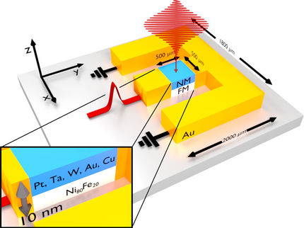
Now, using a new material system, the research team managed to convert a significant part of the intense gigahertz radiation – the incoming radiation had a frequency of 500 gigahertz (GHz) – into the terahertz range. To do so, they combined a so-called topological insulator with gold structures, thereby creating a metamaterial, that is, a material with a tailored structure characterized by special optical, electrical or magnetic properties. In this way, they achieved a conversion efficiency of almost ten percent of the electrical field strength by comparison with roughly one percent previously.
2D electronics, 3D cooling
“We started off using graphene because it has a particular electronic structure that allows electrons to be accelerated very efficiently. But then we observed that at high intensities, graphene reaches its limits,” explains Dr. Jan-Christoph Deinert, co-author of the study, who is also responsible for the terahertz source TELBE. The ultrathin graphene is composed of a single layer of carbon atoms. When a giga- or terahertz pulse hits the material the electron system immediately heats up to several thousand degrees Celsius. In this hot state, however, graphene becomes transparent for the incoming radiation. In order to interact and convert signals the material needs to cool down – and do so within about a trillionth of a second, the oscillation period of the terahertz field. Otherwise, the signal gets lost in the interim.
Since the hot electrons in graphene do not have enough opportunities to shed their excess heat, the researchers next tested the prototype topological insulator bismuth selenide. Internally, topological insulators do not conduct electrical currents, whereas electrons can move freely only at the very surface. Rather like graphene, the electronic signal conversion therefore takes place in two dimensions exclusively on the topmost layer. Unlike graphene, electronic heat can be emitted very quickly via the nearly instantaneous internal interaction with electrons in the bulk of the material. The result is fast 3D cooling instead of 2D heat accumulation.
“Even at room temperature, the system is extremely efficient. And we haven’t yet reached the limits: we can probably even increase the performance for higher intensities,” estimates Dr. Georgy Astakhov, head of the Quantum Materials and Technology Department at HZDR’s Institute for Ion Beam Physics and Materials Research and one of the initiators of the study.
“Material Lego” to reach optimum performance
The high radiation intensities on the sample are achieved by the vapor deposition of gold on the topological insulators. Just like little antennas, they locally enhance the incoming electric fields. “We had already used this approach on graphene. Now we are combining the antenna structures with topological insulators. It’s a bit like material Lego,” says Klaas-Jan Tielrooij whose team in Barcelona applies the gold structures. The topological insulators have been grown in dedicated laboratories in Würzburg, in the context of a collaboration with the ct.qmat Cluster of Excellence that studies new materials and exotic quantum phenomena.
The next step the researchers want to take is to optimize the newly constructed metamaterial prototypes: they want to understand better which parameters are decisive, up to what radiation intensity the process functions, and whether graphene and topological insulators can be functionally combined. Above all, they want to continue improving the system with an eye to possible applications and test realistic conditions so that, one day, they can be integrated into common semiconductor technology.
Original publication
K.-J. Tielrooij, A. Principi, D. S. Reig, A. Block, S. Varghese, S. Schreyeck, K. Brunner, G. Karczewski, I. Ilyakov, O. Ponomaryov, T. V. A. G. de Oliveira, M. Chen, J.-C. Deinert, C. G. Carbonell, S. O. Valenzuela, L. W. Molenkamp, T. Kiessling, G. V. Astakhov, S. Kovalev: "Milliwatt terahertz harmonic generation from topological insulator metamaterials"; Light: Science & Applications, 2022.
