Green electronics made from wood
Sensors and actuators of the future
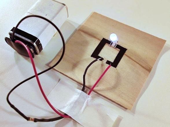
Sustainable electronic components can be made from wood with the help of a novel process that uses a laser to engrave electrically conductive structures on veneers. A research team at Empa and at ETH’s Institute for Building Materials has developed a practical and versatile method for making wooden surfaces electrically conductive.

Green electronics: Making electronic components at least partly from a natural raw material like wood seems an obvious solution.
SNF
Non-biodegradable electronic waste continues to accumulate year after year. For that reason, making electronic components at least partly from a natural raw material like wood seems an obvious solution. But it’s easier said than done. For one thing, wood is naturally an electrical insulator. It also has a complex structure, making it a challenge to achieve homogeneous electrical properties during large-scale fabrication.
Now, a research team at Empa and at ETH’s Institute for Building Materials has developed a practical and versatile method for making wooden surfaces electrically conductive by graphitising them. In this way, devices such as touch panels and sensors can be produced on a large scale with great efficiency. The trick is to pretreat the wood with an ink containing iron. The project, led by Ingo Burgert and Guido Panzarasa, was supported by the Swiss National Science Foundation.
Ink from the Middle Ages
To make conductive structures on wood, the new method improves an existing process called laser-induced graphitization. A laser can engrave fine lines into wooden boards, or veneers. In this process, the energy of the laser beam heats the wood, causing a series of pyrolytic events leading to the formation of electrically conductive graphite. However, the obtained conductive patterns are irregular in depth and width, and there is also a fire hazard due to overheating. Often, multiple post-processing laser steps are needed as well. “The density of wood varies depending on the tree species and growth,” says Christopher Dreimol, first author of the study. “The result can be very uneven graphitization.”
The research team thus came up with the idea of using iron as a catalyst to enable a gentler process and a much more homogeneous surface. Searching for a biologically based catalyst material, Dreimol was inspired by the iron-gall ink, a mixture of iron salt and tannins used as early as the Middle Ages for writing. After optimizing the recipe, Dreimol coated a variety of wood veneers with a thin layer of the ink and then subjected them to the laser treatment.
The ink layer had the desired effect. The patterns engraved after just one pass showed a more uniform structure and conductivity, regardless of differences in the wood structure and type. “Because of the ink, the wood is transformed so quickly into graphite that there is less thermal damage and no risk of fire,” says Dreimol. In addition, much less wood is ablated. The patterns are only a few micrometers deep and can thus be engraved into the thinnest veneer without actually damaging it.
Luminescent wood for displays
The team then used their new method to produce trial electronic components from spruce, cherry and beech veneers less than half a millimeter thick. According to Dreimol, bendable strain sensors could be integrated discreetly into load-bearing wood components in buildings, allowing for constant monitoring of their structural health. The researchers were also able to make the wafer-thin wood glow by means of an electroluminescent layer. Despite the grain of the veneer, homogeneous illumination was achieved. This is an unprecedented result and could be used in applications such as backlighting for displays or for advertisements and control panels. For the electroluminescent wood, the researchers used still conventional wiring and electronic components, however. In the future, these could also be partially replaced by conductive wood.
The next step is to refine and further develop the method for large-scale use: “The fact that we can now process relatively large areas in an acceptable amount of time is the first step towards industrializing electronic components made of wood,” says Dreimol.


