3D Laser Nanoprinters Become Compact
Researchers Show How 3-dimensional Nanostructures Can Be Printed Using Compact Desktop Devices
Lasers in conventional laser printers for paper printouts are very small. 3D laser printers for 3-dimensional microstructures and nanostructures, by contrast, have required big and expensive laser systems so far. Researchers of Karlsruhe Institute of Technology (KIT) and the Heidelberg University now use another process for this purpose. Two-step absorption works with inexpensive and small, blue laser diodes. As a result, much smaller printers can be used.
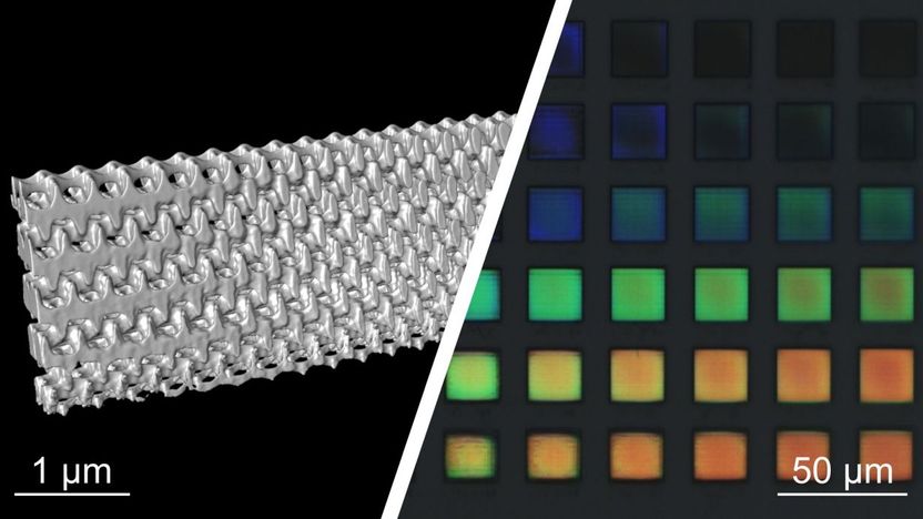
Electron microscopic reconstruction of a 3D nanostructure printed with the 2-step absorption process (left) and light microscopy (right).
Professor Rasmus Schröder, University of Heidelberg, Vincent Hahn, KIT
Presently, laser printing is the method of choice for additive manufacture by 3D printing, as it offers the best spatial resolution of all methods and reaches an extremely high printing speed. In laser printing, a focused laser beam is directed towards a light-sensitive liquid. At the focal point, the laser light turns a switch in special molecules and triggers a chemical reaction. The reaction leads to the local hardening of the material. By moving the focal point, any 3D micro- and nanostructures can be produced. The chemical reaction is based on so-called two-photon absorption, meaning that two photons excite the molecule at the same time, which causes the desired chemical modification. However, this simultaneous excitation happens very rarely, which is why complex pulsed laser systems have to be applied, resulting in bigger dimensions of the laser printer.
More Compact 3D Printers Thanks to Two-step Process
When using the so-called two-step process, more compact, smaller printers can be realized. The first photon transfers the molecule to an intermediate state. In the second step, a second photon transfers the molecule from the intermediate state to the desired excited state and starts chemical reaction. The advantage: Contrary to two-photon absorption, the absorption of the two photons must not necessarily happen at the same time. “For the process, compact and low-power continuous-wave laser diodes can be used,” says Vincent Hahn, the first author of the study from KIT’s Institute of Applied Physics (APH). The required laser powers are far below those of conventional laser pointers. Printing, however, requires specific photoresists. “Development of these photoresists has taken several years and has been possible only in collaboration with chemists,” says Professor Martin Wegener, APH.
Not Only Easier, but Better
“The publication reveals that the idea works, even better than the previously used two-photon absorption,” Hahn says. To Martin Wegener, the advantage is obvious: “It is a big difference between using a femtosecond laser as large as a big suitcase for several ten thousand euros or a semiconductor laser that is as large as a pinhead and costs less than ten euros. Now, the other components of the 3D laser nanoprinter also have to be miniaturized. To me, a device that will be as large as a shoebox appears realistic in the next years. That would be even smaller than the laser printer on my desktop at KIT.” This way, 3D laser nanoprinters might become affordable for many groups. Experts are already talking about a democratization of 3D laser printing technology.
Along with KIT researchers, scientists from Heidelberg University were involved in the publication. The publication originated within the framework of the joint Cluster of Excellence "3D Matter Made to Order" of KIT and Heidelberg University.
Original publication
Most read news
Original publication
V. Hahn, T. Messer, M. Bojanowski, E.R. Curticean, I. Wacker, R. Schröder, E. Blasco, and M. Wegener; "Two-step absorption instead of two-photon absorption in 3D laser nanoprinting"; Nature Photonics; 2021
Organizations
Other news from the department science

Get the chemical industry in your inbox
By submitting this form you agree that LUMITOS AG will send you the newsletter(s) selected above by email. Your data will not be passed on to third parties. Your data will be stored and processed in accordance with our data protection regulations. LUMITOS may contact you by email for the purpose of advertising or market and opinion surveys. You can revoke your consent at any time without giving reasons to LUMITOS AG, Ernst-Augustin-Str. 2, 12489 Berlin, Germany or by e-mail at revoke@lumitos.com with effect for the future. In addition, each email contains a link to unsubscribe from the corresponding newsletter.
Most read news
More news from our other portals
Last viewed contents
First high-resolution images of bone, tooth and shell formation
