Researchers move closer to controlling two-dimensional graphene
The device you are currently reading this article on was born from the silicon revolution. To build modern electrical circuits, researchers control silicon’s current-conducting capabilities via doping, which is a process that introduces either negatively charged electrons or positively charged "holes" where electrons used to be. This allows the flow of electricity to be controlled and for silicon involves injecting other atomic elements that can adjust electrons— known as dopants—into its three-dimensional (3D) atomic lattice.

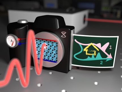
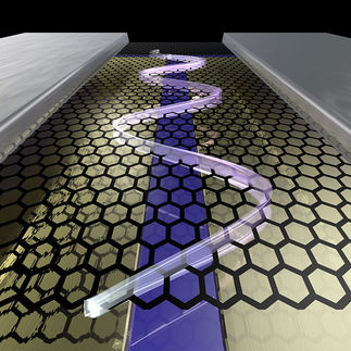
The TOS-doped graphene is highly conductive but absorbs very little of the infrared light in the resonator—a combination of properties that makes this material unique and promising for opto-electronic applications.
Ipshita Datta, Lipson Nanophotonics Group, Columbia University
Silicon’s 3D lattice, however, is too big for next-generation electronics, which include ultra-thin transistors, new devices for optical communication, and flexible bio-sensors that can be worn or implanted in the human body. To slim things down, researchers are experimenting with materials no thicker than a single sheet of atoms, such as graphene. But the tried-and-true method for doping 3D silicon doesn’t work with 2D graphene, which consists of a single layer of carbon atoms that doesn’t normally conduct a current.
Rather than injecting dopants, researchers have tried layering on a "charge-transfer layer" intended to add or pull away electrons from the graphene. However, previous methods used "dirty" materials in their charge-transfer layers; impurities in these would leave the graphene unevenly doped and impede its ability to conduct electricity.
Now, a new study in Nature Electronics proposes a better way. An interdisciplinary team of researchers, led by James Hone and James Teherani at Columbia University, and Won Jong Yoo at Sungkyungkwan University in Korea, describe a clean technique to dope graphene via a charge-transfer layer made of low-impurity tungsten oxyselenide (TOS).
The team generated the new "clean" layer by oxidizing a single atomic layer of another 2D material, tungsten selenide. When TOS was layered on top of graphene, they found that it left the graphene riddled with electricity-conducting holes. Those holes could be fine-tuned to better control the materials’ electricity-conducting properties by adding a few atomic layers of tungsten selenide in between the TOS and the graphene.
The researchers found that graphene’s electrical mobility, or how easily charges move through it, was higher with their new doping method than previous attempts. Adding tungsten selenide spacers further increased the mobility to the point where the effect of the TOS becomes negligible, leaving mobility to be determined by the intrinsic properties of graphene itself. This combination of high doping and high mobility gives graphene greater electrical conductivity than that of highly conductive metals like copper and gold.
As the doped graphene got better at conducting electricity, it also became more transparent, the researchers said. This is due to Pauli blocking, a phenomenon where charges manipulated by doping block the material from absorbing light. At the infrared wavelengths used in telecommunications, the graphene became more than 99 percent transparent. Achieving a high rate of transparency and conductivity is crucial to moving information through light-based photonic devices. If too much light is absorbed, information gets lost. The team found a much smaller loss for TOS-doped graphene than for other conductors, suggesting that this method could hold potential for next-generation ultra-efficient photonic devices.
“This is a new way to tailor the properties of graphene on demand,” Hone said. “We have just begun to explore the possibilities of this new technique.”
One promising direction is to alter graphene’s electronic and optical properties by changing the pattern of the TOS, and to imprint electrical circuits directly on the graphene itself. The team is also working to integrate the doped material into novel photonic devices, with potential applications in transparent electronics, telecommunications systems, and quantum computers.
Original publication
Most read news
Other news from the department science

Get the chemical industry in your inbox
By submitting this form you agree that LUMITOS AG will send you the newsletter(s) selected above by email. Your data will not be passed on to third parties. Your data will be stored and processed in accordance with our data protection regulations. LUMITOS may contact you by email for the purpose of advertising or market and opinion surveys. You can revoke your consent at any time without giving reasons to LUMITOS AG, Ernst-Augustin-Str. 2, 12489 Berlin, Germany or by e-mail at revoke@lumitos.com with effect for the future. In addition, each email contains a link to unsubscribe from the corresponding newsletter.
Most read news
More news from our other portals
Last viewed contents
Protactinium
Wireless_energy_transfer
Phosphazene
Chlorargyrite
Pasteurization
Cresol
Vanabins


